


LMH6551 Differential Amplifier: 7 Checks for a Balanced ADC Path

LMH6551 Differential Amplifier: 7 Checks for a Balanced ADC Path
Check LMH6551 feedback balance, input common mode, output bias and ADC loading before trusting a differential acquisition path. This is a documentation-based planning guide, not a report of independent hands-on testing.
1. Specify differential and common-mode signals separately
The LMH6551 is a voltage-feedback differential amplifier used for ADC driving and balanced signal paths. Define input format, required differential gain, output amplitude and receiving-circuit bias before selecting resistor values. Two outputs form one differential path, but each output must remain within its own valid operating range. Draw the differential voltage and the average output voltage as separate quantities. This prevents a plausible gain calculation from hiding an incompatible output common mode or a clipped individual waveform. Manufacturer documentation.
2. Preserve symmetry in both feedback networks
Use the manufacturer equations for differential gain and the associated resistor networks. Ratio matching matters because imbalance can convert signal energy into unwanted common-mode movement and degrade distortion. Include the source impedance, including any termination resistance, when selecting or matching the input network. Keep feedback components close to the amplifier and avoid unequal parasitic paths. A collection of nominally identical resistor values does not establish balance if one input sees additional series impedance from a cable or sensor output. Manufacturer documentation.
3. Check input common mode for the complete topology
Single-ended-to-differential conversion does not mean the unused side can be connected arbitrarily without affecting the operating point. The feedback action determines the amplifier input voltages, and the allowed range depends on supply conditions. Calculate those voltages for both extremes of the intended signal. Review the single-supply application guidance if ground-referenced sources are involved. A signal safely inside the eventual ADC range may still force the amplifier input stage outside its linear region before reaching that converter. Manufacturer documentation.
4. Set VCM using a suitable analog reference
The VCM pin controls output common mode and has a finite input impedance. If left at its documented default bias, confirm that the resulting midpoint suits the receiving circuit; otherwise drive it using the specified approach. Check reference-source loading, noise and stability rather than treating VCM as a digital mode pin. Include VCM settling in startup qualification. A correct average output at no load does not prove that the reference path remains quiet while a converter repeatedly charges its sampling network. Manufacturer documentation.
Newest in the store


5. Interpret speed and distortion under matching conditions
The datasheet presents high small-signal bandwidth and fast slew performance with specified gain, load, supply and amplitude. Those figures do not establish identical response for every closed-loop circuit. Assess full-power bandwidth and settling for the actual differential swing, not only a tiny sine wave. Compare expected distortion under realistic loading and common mode. Keep typical characterization separate from guaranteed limits in the design record, and do not report manufacturer plots as measurements independently obtained from the assembled board. Manufacturer documentation.
6. Isolate capacitive loading without losing acquisition accuracy
An ADC input can be a dynamic capacitive load rather than a fixed resistor. Follow the capacitive-drive and converter-interface guidance when adding series resistance or filtering. Then account for the resulting settling time and any attenuation in the gain calculation. Differential symmetry still matters: mismatched output networks can introduce imbalance even when the amplifier feedback resistors are matched. Probe carefully because unequal or high-capacitance probes can change the behavior being investigated and create an apparent channel fault. Manufacturer documentation.
7. Qualify balance before connecting an unknown signal
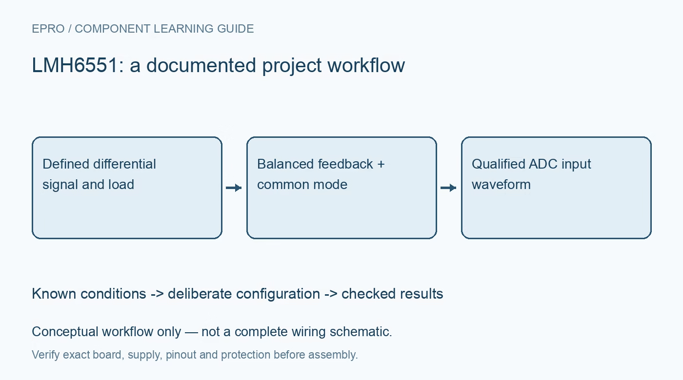
Start with defined supplies, the intended VCM reference and a bounded known input. Check both output waveforms, their average and their difference across a useful frequency and amplitude range. Include startup, load changes and any clipping recovery that the application may encounter without exceeding device limits. Save resistor ratios, source impedance, output network and measurement loading with the results. The objective is a reproducible balanced signal path, not a blanket claim of headline bandwidth or distortion on an unspecified module. Manufacturer documentation.
Related reading: OPA855 Bipolar Amplifier: 7 Checks for Noise Gain and Bias Current.
Catalog note: The exact-part search did not return a matching Epro listing during preparation. Check the current catalog; this guide makes no price, availability or included-accessory claim.