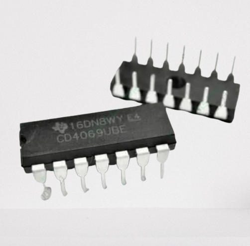
CD4069 Hex Inverter IC (NOT Gate) – DIP-14
The CD4069 is a hex inverter IC that contains six independent NOT gates (inverters). This device is designed to provide logic inversion for digital signals, making it a versatile component for a wide range of digital electronics applications. Each gate has a single input and a single output, providing the inverse of the input signal.
Key Features:
- Hex Inverter (6 Gates): Contains six independent inverters, making it suitable for applications requiring multiple signal inversions.
- CMOS Technology: The CD4069 is built using CMOS (Complementary Metal-Oxide-Semiconductor) technology, offering low power consumption and high noise immunity.
- Wide Voltage Supply Range: It operates with a broad voltage supply range from 3V to 15V, making it compatible with various systems and voltage levels.
- Low Power Consumption: Being a CMOS IC, it offers very low static power dissipation, ensuring energy efficiency for both battery-powered and high-performance systems.
- Standard Pin Configuration (DIP-14 Package): The device comes in a DIP-14 package, which is ideal for breadboards and general prototyping.
- High Noise Immunity: The CMOS construction ensures robust performance in environments with electrical noise or interference.
Electrical Characteristics:
- Supply Voltage (Vcc): 3V to 15V
- Input Voltage (Vi): 0V to Vcc
- Output Voltage (Vo): 0V to Vcc
- Input Current (Iin): 1 µA (max)
- Output Drive Capability: Can drive up to 5mA of current.
- High Noise Immunity: Due to CMOS technology, this IC exhibits high noise immunity, making it resistant to interference from other electronic signals.
- Operating Temperature Range: -55°C to +125°C
Pin Configuration (DIP-14 Package):
- Pin 1 (Input 1) – First input of the first inverter.
- Pin 2 (Output 1) – Output of the first inverter.
- Pin 3 (Input 2) – Input of the second inverter.
- Pin 4 (Output 2) – Output of the second inverter.
- Pin 5 (Input 3) – Input of the third inverter.
- Pin 6 (Output 3) – Output of the third inverter.
- Pin 7 (Ground) – Ground pin.
- Pin 8 (Input 4) – Input of the fourth inverter.
- Pin 9 (Output 4) – Output of the fourth inverter.
- Pin 10 (Input 5) – Input of the fifth inverter.
- Pin 11 (Output 5) – Output of the fifth inverter.
- Pin 12 (Input 6) – Input of the sixth inverter.
- Pin 13 (Output 6) – Output of the sixth inverter.
- Pin 14 (Vcc) – Supply voltage pin.
Applications:
- Logic Circuits: The CD4069 is commonly used for implementing NOT logic in combinational logic circuits.
- Signal Inversion: It is used to invert digital signals in various circuits, such as signal processing systems, oscillators, and logic gates.
- Pulse Shaping: The inverter can be used for pulse shaping or signal timing applications.
- Battery-Powered Applications: Due to its low power consumption, the CD4069 is ideal for portable or battery-operated devices.
- Signal Processing: The device is often used in circuits that require the inversion of signals, such as amplifiers and pulse modulation systems.
Advantages:
- Energy-Efficient: Its low power consumption makes it ideal for energy-conscious designs.
- Multiple Gates in One Package: The IC contains six inverters in a single package, providing space-saving and cost-effective benefits for circuits requiring multiple NOT gates.
- Wide Voltage Range: The device can be used across various voltage levels, making it versatile for a wide range of applications.
- Easy Integration: The standard 14-pin DIP package makes it easy to integrate into both through-hole and surface-mount designs.
Package Includes:
- 1 x CD4069 Hex Inverter NOT Gate IC (DIP-14 Package)
The CD4069 Hex Inverter is a versatile and efficient choice for various digital logic applications. Whether you’re building simple inverters or need a reliable IC for signal processing, this IC offers flexibility, low power consumption, and ease of use for both amateur and professional engineers.



Awais Javed (verified owner) –
High quality and reliable. Thank you! (From Lahore)
Saad Farooq (verified owner) –
Really happy with the quality. Recommended! (From Quetta)
Awais Javed (verified owner) –
Excellent product, exactly as described! (From Peshawar)
Ahmed Khan (verified owner) –
Excellent product, exactly as described! (From Quetta)
Faizan Malik (verified owner) –
Good packaging and fast delivery. (From Sargodha)
Usman Raza (verified owner) –
Totally satisfied with the purchase. (From Abbottabad)