


ADS1018 SPI ADC: 7 Checks Before Scaling a Conversion

ADS1018 SPI ADC: 7 Checks Before Scaling a Conversion
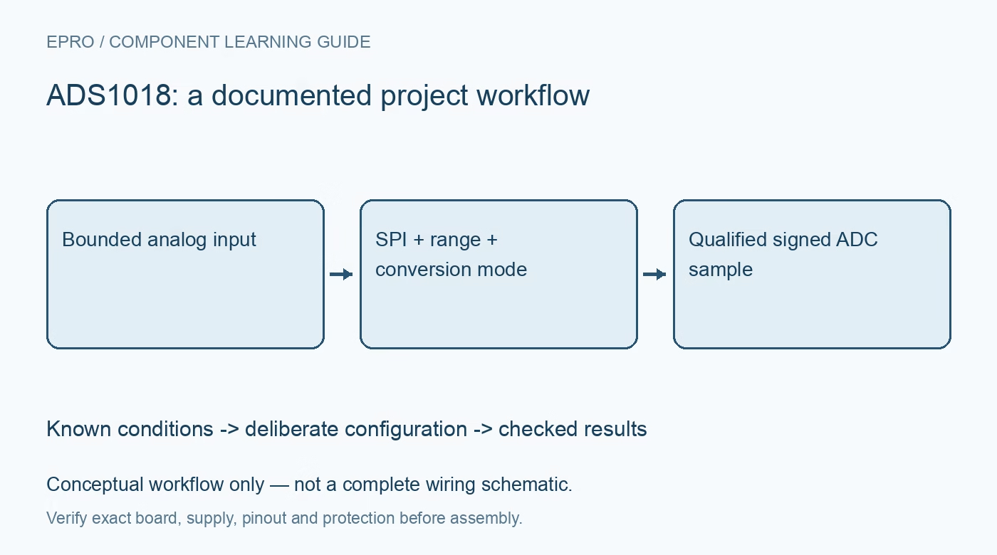
Plan ADS1018 acquisition with correct 12-bit alignment, SPI framing, PGA input limits, fresh conversion handling and explicit temperature-mode switching. This is a documentation-based planning guide, not a report of independent hands-on testing.
1. Keep the ADS1018 resolution distinct
ADS1018 is a 12-bit delta-sigma ADC with an input multiplexer, programmable gain and an internal temperature-sensing mode. Do not inherit the resolution assumptions of a similarly named 16-bit device. Identify the actual part and carrier before selecting a library or conversion constant. Multiple input pins do not imply simultaneous independent converters. Define the required differential or single-ended measurement and preserve that selection with the configuration used to interpret each accepted sample. Manufacturer documentation.
2. Check absolute input voltages first
Review the voltage at every analog input as well as the desired differential signal. A programmable full-scale range is a numerical conversion range, not permission to exceed the input-pin limits set by the supplies and documentation. Include source impedance, protection and grounding in the circuit assessment. Keep introductory evaluation suitably protected and low voltage. Neither differential acquisition nor a wide PGA setting makes the device an isolated instrument appropriate for direct hazardous-voltage measurements. Manufacturer documentation.
3. Choose gain and scaling together
Select the PGA range from the expected signal and its credible variation, then use the documented transfer relationship for the installed device. Predict clipping before attaching the intended load or sensor. Preserve gain and reference assumptions beside raw codes. Do not change a software multiplier to make an out-of-range or miswired signal look correct. The integrated reference simplifies the design, but it does not remove source, wiring, ADC offset and gain contributions from a complete accuracy assessment. Manufacturer documentation.
4. Implement the documented SPI sequence
Verify clocking, chip select, data direction, command framing and configuration behavior using the exact device documentation. Review the shared data-ready function where relevant to the host implementation. A peripheral transfer completing without a host error does not establish that a fresh conversion was returned or that the requested configuration took effect. Retain raw transmitted and received words during evaluation so an interface-timing or framing issue can be separated from an analog input limitation. Manufacturer documentation.
Newest in the store


5. Decode the aligned signed result
The meaningful conversion information occupies the documented field within the serial result word. Apply the correct alignment, sign handling and scaling rather than treating every transferred bit as additional resolution. Check negative, zero and positive numerical cases explicitly. A mistake can remain hidden when only a small positive voltage is tried. Preserve the original word and decoded count alongside engineering values while evaluating the driver instead of relying solely on a rounded display. Manufacturer documentation.
6. Separate external-input and temperature modes
The internal temperature mode observes the device’s thermal condition; it is not a separate external temperature probe. Track mode changes explicitly and accept data only after the relevant conversion sequence. Do not apply an analog-voltage equation to a temperature result or assume the first word after a configuration change represents the newly selected input. For thermocouple-related work, sensor placement, cold-junction conditions and the external sensor model remain separate engineering responsibilities beyond enabling the integrated temperature feature. Manufacturer documentation.
7. Keep timing and validity in the record
Retain part identity, input selection, PGA range, conversion mode, data rate, raw result and acquisition time with observations. Evaluate the completed chain against suitable reference equipment before claiming accuracy or useful noise-free resolution. The linked ADS1118 guide addresses a different resolution and does not provide interchangeable output interpretation. This ADS1018 workflow proposes traceable acquisition checks and claims no independent physical measurements, universal library compatibility or finished temperature-instrument performance from the ADC feature list alone. Manufacturer documentation.
Related reading: ADS1118 ADC: 7 Checks for SPI, Input Range and Temperature Mode.
Catalog note: The exact-part search did not return a matching Epro listing during preparation. Check the current catalog; this guide makes no price, availability or included-accessory claim.