


ADS8866 SAR ADC: 7 Checks for CONVST Mode and Input Settling

ADS8866 SAR ADC: 7 Checks for CONVST Mode and Input Settling
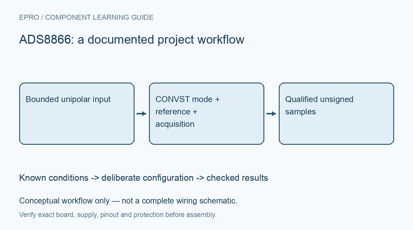
Plan ADS8866 sampling with explicit CONVST and DIN behavior, near-ground negative input limits, reference drive and unsigned 16-bit decoding. This is a documentation-based planning guide, not a report of independent hands-on testing.
1. Define a unipolar measurement rather than a generic differential one
ADS8866 is a sixteen-bit, one-hundred-kilosample-per-second SAR ADC with a unipolar single-ended input span. Although it exposes AINP and AINN, the negative input has a tightly constrained near-ground operating range; it is not an unrestricted differential sensor interface. Check both individual input voltages and the AINP-minus-AINN span against the electrical table. Begin with a bounded known source. The pin names alone do not establish compatibility with a floating bridge or a bipolar signal. Manufacturer documentation.
2. Map analog supply, logic supply and reference separately
The device has separate AVDD and DVDD requirements and uses an external reference with its own specified range. The allowed reference voltage is independent of the analog supply under the documented conditions, so do not substitute a generic rule from another ADC. Verify every pin against recommended operation and absolute limits. Add local decoupling and check the host logic interface at the chosen DVDD. An acceptable reference voltage does not establish that the analog or digital supplies are correct. Manufacturer documentation.
3. Select interface mode through the actual DIN connection
DIN at the CONVST rising edge determines whether the converter uses the applicable chip-select mode or daisy-chain mode. Document the hardware connection and intended three-wire or four-wire operation before implementing SPI transfers. In three-wire operation, CONVST also serves the chip-select function; in the other supported arrangement, sampling can be controlled separately from serial timing. Use the relevant timing diagram rather than treating every pin-count option as an interchangeable software setting. Manufacturer documentation.
4. Budget acquisition and conversion intervals explicitly
A no-latency output does not mean conversion takes no time or that the analog source settles instantaneously. Establish the sampling instant, conversion interval, acquisition interval and allowed serial-clock activity from the selected timing diagram. Check minimum high and low times and the required separation of events at the pins. Timestamp the actual acquisition schedule rather than host read completion. A plausible sequence of changing words can still come from a mis-timed transaction or an incompletely settled input. Manufacturer documentation.
Newest in the store


5. Drive the sampled input and reference dynamically
The input sample-and-hold network and the reference input draw dynamic charge, so evaluate source impedance, the driver and local capacitor network together. Follow the manufacturer application guidance for bandwidth, filtering and reference drive at the intended sample rate. Do not qualify the chain using only average current or a stationary meter reading. Start with a slow bounded stimulus and increase acquisition demand deliberately. A precision source can still produce conversion error if the chosen network cannot settle in time. Manufacturer documentation.
6. Decode straight binary without borrowing signed-ADC logic
ADS8866 output data is straight binary across the unipolar span. Extract the correct sixteen data bits and apply the documented transfer function using the actual reference voltage. Do not sign-extend the most significant bit as though this were a bipolar two’s-complement delta-sigma converter. Test synthetic zero, midscale and near-full-scale values in the software first. Treat clipping as a limit condition, not a valid extrapolated voltage, and retain raw codes so scaling problems remain diagnosable. Manufacturer documentation.
7. Qualify codes, timing and error as separate requirements
Compare results against several known input points after the reference and input chain settle. Record raw words, reference value, interface mode, CONVST timing, serial-clock settings and input-drive network. Assess offset, gain, noise and linearity separately from transport success. A nominal sixteen-bit result does not guarantee sixteen-bit system accuracy. This documentation-based plan does not report independent measurements; recheck the relevant timing and settling evidence whenever the host clock, sample rate, driver or reference arrangement changes. Manufacturer documentation.
Related reading: ADS127L01 ADC: 7 Checks for Filter Timing and Valid Data Frames.
Catalog note: The exact-part search did not return a matching Epro listing during preparation. Check the current catalog; this guide makes no price, availability or included-accessory claim.