


TPS27082L Load Switch: 7 Checks for Slew Rate and Inrush

TPS27082L Load Switch: 7 Checks for Slew Rate and Inrush
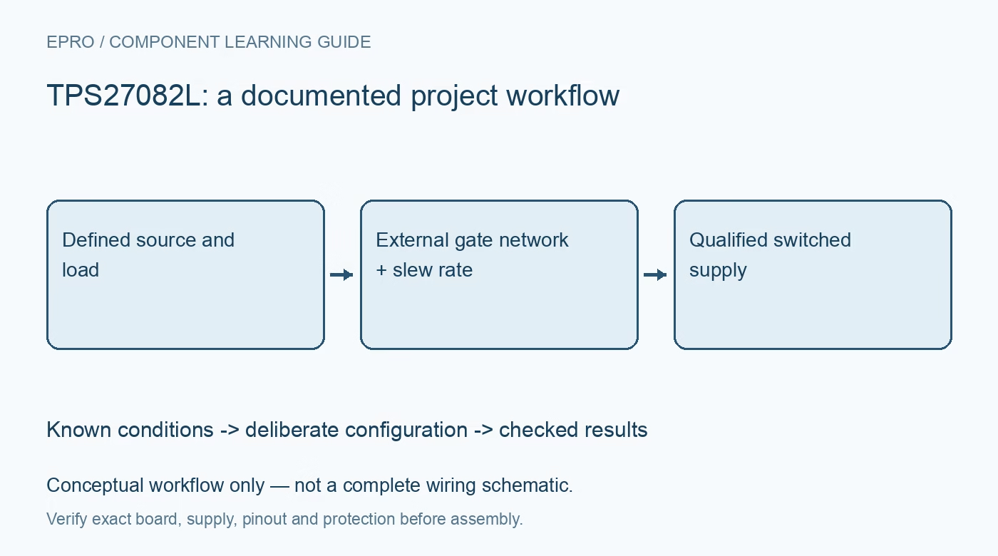
Review TPS27082L load-switch design with the correct external gate network, controlled rise time, logic limits and realistic inrush and protection expectations. This is a documentation-based planning guide, not a report of independent hands-on testing.
1. Separate a load switch from a protected power controller
TPS27082L integrates a high-side PFET and control circuitry for switching a supply to a load. Its documented operating range extends from 1.2 V to 8 V, with load capability dependent on the actual electrical and thermal conditions. It is not a DC converter. Do not infer programmable current limiting, fault telemetry or comprehensive reverse-current blocking merely from the load-switch label. List required protections separately and provide external measures where the design needs them. Manufacturer documentation.
2. Reconstruct the external network from the exact schematic
The VIN, VOUT, ON/OFF and R1/C1 connections are not interchangeable with similarly sized six-pin switches. Follow the manufacturer typical application and pin table together, including the intended ground connection and external pull-up resistor. An optional capacitor controls switching behavior through the gate network; it is not simply another output bypass capacitor. Check the assembled board with power removed. A package photograph or a generic three-terminal switch drawing cannot establish the missing connections. Manufacturer documentation.
3. Include the resistor network in the conduction-loss budget
The external pull-up and internal control resistance affect the PFET gate-source drive, which in turn affects on-resistance. Do not budget the lowest headline resistance at every supply voltage or resistor choice. Estimate voltage drop and dissipation using the appropriate operating conditions and temperature behavior. A larger load may heat a small package substantially even when the current is below a headline maximum. Verify trace width, connectors and return paths alongside the silicon. Manufacturer documentation.
4. Size slew control around capacitance and source capability
Charging a load capacitor requires current approximately equal to capacitance times voltage slew rate, in addition to any current consumed by the active load. Slowing the output ramp can reduce inrush, but it does not impose a universal hard current limit. Use the documented network and curves to establish an initial design, then measure the real ramp. Include downstream startup behavior because some loads begin drawing substantial current before the switched rail has reached its final value. Manufacturer documentation.
Newest in the store




5. Make enable logic deterministic across power sequencing
Review ON/OFF thresholds, hysteresis and recommended pin conditions with the actual host voltage. Establish the intended state while the microcontroller resets, loses power or configures its GPIO. A logic output that is temporarily high impedance is not a guaranteed command. Avoid driving unpowered nodes outside their permitted conditions. Check whether external biasing affects standby current or backfeeds another rail. The control-interface convenience does not remove the need for an explicit sequencing plan. Manufacturer documentation.
6. Check turnoff and transients without assuming isolation features
Measure the load-side voltage after disable and determine how stored output energy is removed. Do not assume an active discharge feature or a guaranteed discharge time unless the exact implementation provides it. Consider externally driven loads and inductive wiring separately; capacitors and cable inductance can create overshoot. The documented fast input-transient isolation behavior is not a blanket guarantee for every reverse-powered scenario. Use current-limited tests and suitable external protection rather than destructive short-circuit experiments. Manufacturer documentation.
7. Approve switching behavior with a repeatable load record
Log input voltage, capacitance, active-load profile, external resistor and capacitor values, rise time, droop and package temperature. Exercise repeated enable cycles after the rail has both fully and partly discharged. Compare the observed behavior with the source current limit and downstream reset requirements. Retain a schematic-level explanation of every external component. This is a planning guide derived from the manufacturer documentation; a final current rating or timing guarantee requires validation of the actual board and its operating environment. Manufacturer documentation.
Related reading: TPS22918 Load Switch: 7 Checks for an Orderly Sensor Rail.
Catalog note: The exact-part search did not return a matching Epro listing during preparation. Check the current catalog; this guide makes no price, availability or included-accessory claim.