


UCC27624 Gate Driver: 7 Checks for Negative Inputs and Transient Output Limits

UCC27624 Gate Driver: 7 Checks for Negative Inputs and Transient Output Limits
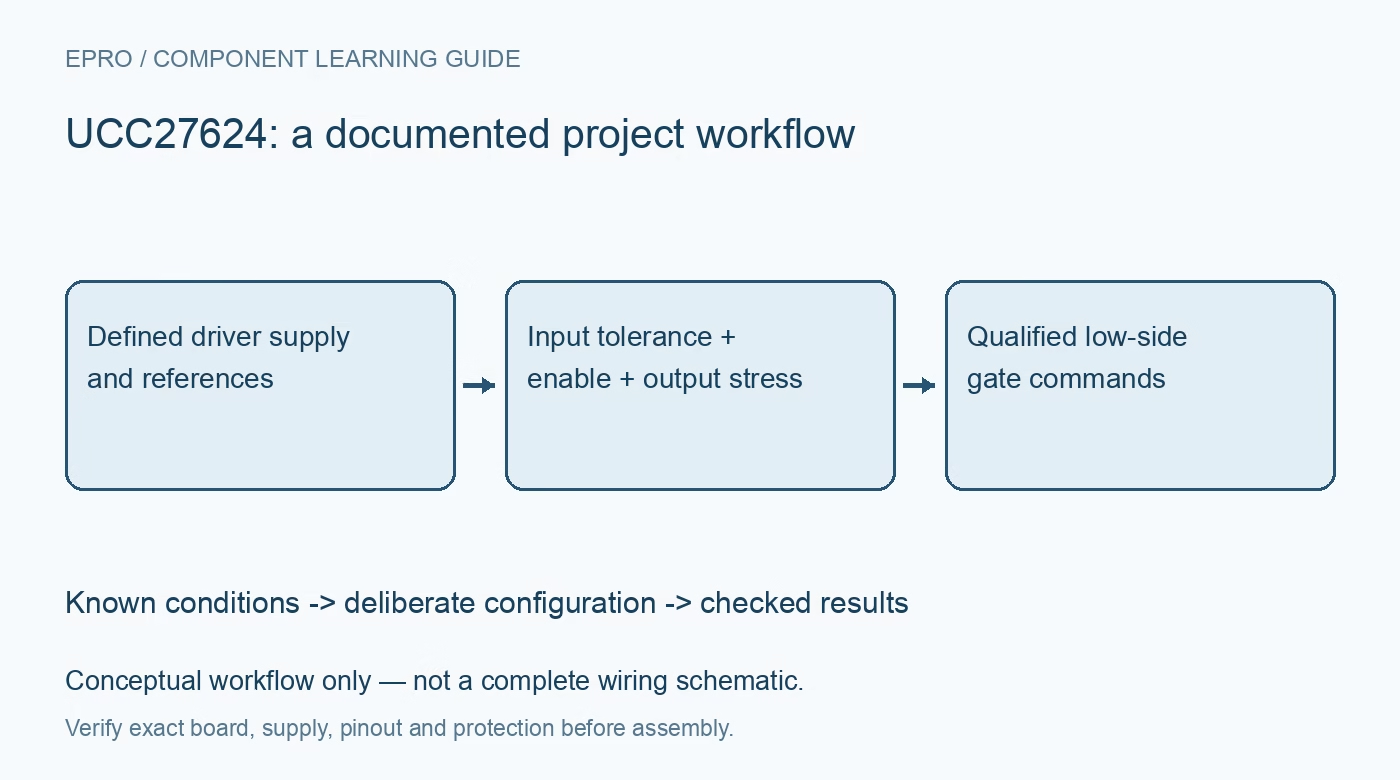
Check UCC27624 input robustness without confusing 30-volt stress ratings, 26-volt operation, enable defaults or transient output limits. This is a documentation-based planning guide, not a report of independent hands-on testing.
1. Separate operating voltage from the absolute maximum
The UCC27624 is a dual noninverting low-side driver with a recommended supply range of 4.5 to 26 volts. Its thirty-volt absolute maximum supply rating is not a recommended thirty-volt operating point. Confirm the exact package, return reference and transistor gate requirements before choosing a bias rail. For initial qualification, disconnect the switching power stage and use benign capacitive gate-equivalent loads with a current-limited low-voltage supply. Driver robustness does not establish a safe high-voltage converter or motor-drive topology. Manufacturer documentation.
2. Apply negative-input capability to the correct terminals
The recommended input range includes minus ten volts on INA, INB, ENA and ENB under the documented conditions. This helps tolerate ground-related disturbances, but it does not make the complete board immune to arbitrary common-mode events. Check the controller output protection, series components, return wiring and voltage at each driver terminal. Do not deliberately inject large negative pulses into an assembled interface simply to demonstrate a headline rating. A robust driver input can coexist with a vulnerable controller pin upstream. Manufacturer documentation.
3. Distinguish continuous output limits from short transients
Normal output operation is between ground and VDD. The absolute-maximum table separately permits specified output excursions for a 200-nanosecond pulse, including minus two volts at the low end; those transient conditions are not continuous operating limits. Review pulse width, amplitude, repetition and the complete output network rather than accepting an oscilloscope minimum value alone. Gate resistors and compact loops can reduce ringing. A waveform that stays inside a brief stress boundary still needs assessment for reliable normal operation. Manufacturer documentation.
4. Make enable defaults part of the startup design
ENA and ENB are active-high enables with internal pullups. Floating enables therefore permit operation, while floating command inputs are pulled toward an output-low state. These defaults have different purposes and should not be conflated. Specify commands and enables during reset, programming and bias recovery, and compare actual controller levels with the fixed logic thresholds. If two channels are intentionally combined under manufacturer guidance, their enables must be driven together; independent enable states can defeat an otherwise common command arrangement. Manufacturer documentation.
Newest in the store


5. Budget gate charge instead of continuous peak current
The five-amp source and sink figures describe peak output-drive capability, not a continuous five-amp power supply. Estimate average demand from gate charge and switching frequency, then include both channels, quiescent consumption and losses. Place appropriate bypass capacitors close to the device and review the selected package thermal path. A larger gate-drive voltage can increase charge-related power as well as transistor stress. Do not choose the highest available bias merely because it sits within the driver operating range. Manufacturer documentation.
6. Treat matched channels as finite-delay channels
Typical channel matching is very tight, but the device does not supply bridge dead time or an isolation barrier. Controller skew, driver propagation, output loading and power-transistor behavior all contribute to the actual switching relationship. Verify both outputs on a common acquisition using matched, low-loading probes where appropriate. Keep logical complementary commands separate from guaranteed nonoverlap. A clean pair of unloaded traces does not prove that two real power devices cannot conduct simultaneously under temperature, supply or load variation. Manufacturer documentation.
7. Retain a stress and startup qualification record
Record supply tolerance, package, load capacitance, resistance, command levels, enables and measured ringing duration. Capture startup, disable and controlled supply removal with the power stage absent. Label datasheet stress boundaries, recommended operating limits and actual measurements separately. Confirm that recovery produces the intended output-low state before the controller releases normal commands. The useful result is a bounded driver-level qualification, not a claim that negative-input capability, transient tolerance or a fast propagation headline validates the complete switching system. Manufacturer documentation.
Related reading: UCC27524A Gate Driver: 7 Checks for Dual-Channel Timing and Enable States.
Catalog note: The exact-part search did not return a matching Epro listing during preparation. Check the current catalog; this guide makes no price, availability or included-accessory claim.