


OPA828 JFET Op Amp: 7 Checks for Input Headroom and MUX Settling

OPA828 JFET Op Amp: 7 Checks for Input Headroom and MUX Settling
Plan OPA828 precision paths with non-rail-to-rail inputs, package-aware specifications, MUX-friendly behavior and qualified ADC settling. This is a documentation-based planning guide, not a report of independent hands-on testing.
1. Use a supported supply and exact package
OPA828 requires a total supply of 8V to 36V, corresponding to the documented dual-supply range of plus or minus 4V through plus or minus 18V. It is not a direct 3.3V or 5V microcontroller-rail amplifier. Identify the SOIC or HVSSOP package and its pin functions, including thermal-pad requirements where present. Some precision specifications differ by package. Save the complete ordering code rather than combining the most attractive typical values from different versions into one assumed device specification. Manufacturer documentation.
2. Budget input common-mode headroom explicitly
This JFET-input amplifier is not a rail-to-rail input part. The electrical table gives a common-mode range bounded approximately by the negative rail plus 2.5V and the positive rail minus 3.5V under the stated conditions. On a nominal plus-or-minus 5V supply, that leaves a much narrower valid input window than the supply span suggests. Check both amplifier inputs, including transient conditions. Output swing has its own load-dependent limits and must not be inferred from the input range. Manufacturer documentation.
3. Understand what MUX-friendly inputs provide
The input architecture avoids the antiparallel differential-input diodes used in many precision amplifiers, reducing the large input-current disturbance that can occur during multiplexer transitions. This helps a high-impedance source, but it is not permission to violate common-mode, absolute-maximum or supply-sequencing limits. Check source protection and settling for the complete channel transition. A large allowable differential transient and accurate closed-loop operation are different claims. Preserve that distinction when selecting input clamps or deciding which samples to accept after switching. Manufacturer documentation.
4. Evaluate the whole channel-change step
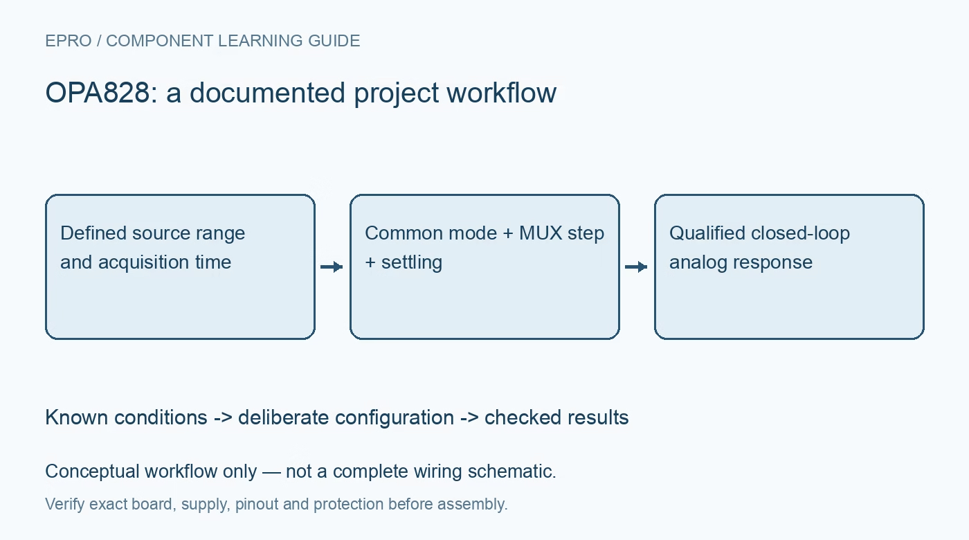
A multiplexer can connect sources with different DC levels and impedances. Include switch charge injection, source recovery, amplifier slew, closed-loop settling and ADC acquisition in the timing budget. The 45MHz gain-bandwidth and 150V-per-microsecond slew-rate headlines describe different behaviors and do not by themselves establish precision settling. Use the documented test conditions and response curves as starting points. Then test the largest intended channel step with the actual feedback network and converter sampling normally. Manufacturer documentation.
Newest in the store


5. Do not generalize the settling headline
The approximately 120ns settling figure is tied to a specified error target, step and circuit condition. It does not guarantee that every high-gain or heavily loaded board is ready for a high-resolution conversion after the same interval. Define the acceptable residual error in volts or converter codes and qualify settling against that requirement. Check for ringing, clipping and recovery, not just the first crossing of the final value. Keep typical characterization separate from guaranteed limits and measured assembled-board performance. Manufacturer documentation.
6. Include source impedance and board leakage
Low JFET input bias current benefits high-impedance sources, but resistor thermal noise, voltage noise, contamination and parasitic capacitance can dominate the result. Model the source and feedback network together, including leakage at temperature. The overload power limiter manages a specific internal power behavior; it does not protect every external sensor or guarantee precision during sustained overload. Keep sensitive nodes clean and compact, and use a layout appropriate to the bandwidth instead of relying on a solderless breadboard for precision high-speed claims. Manufacturer documentation.
7. Preserve a meaningful ADC-drive validation
Use bounded known inputs and a current-limited supply to verify gain, offset, common-mode margin and the response to representative channel changes. Check converter-pin settling during actual acquisition, with any isolation resistor and charge-storage capacitor fitted. Record package, rails, source impedance, feedback values, channel-step size, sampling timing, temperature and probe arrangement. Flag unsettled or saturated conversions rather than averaging them into a plausible result. The final evidence should describe a qualified signal path, not a universal performance promise based on one amplifier headline. Manufacturer documentation.
Related reading: OPA810 FET-Input Op Amp: 7 Checks for Bandwidth, Headroom and ADC Drive.
Catalog note: The exact-part search did not return a matching Epro listing during preparation. Check the current catalog; this guide makes no price, availability or included-accessory claim.