


Understanding the Basics of Printed Circuit Board

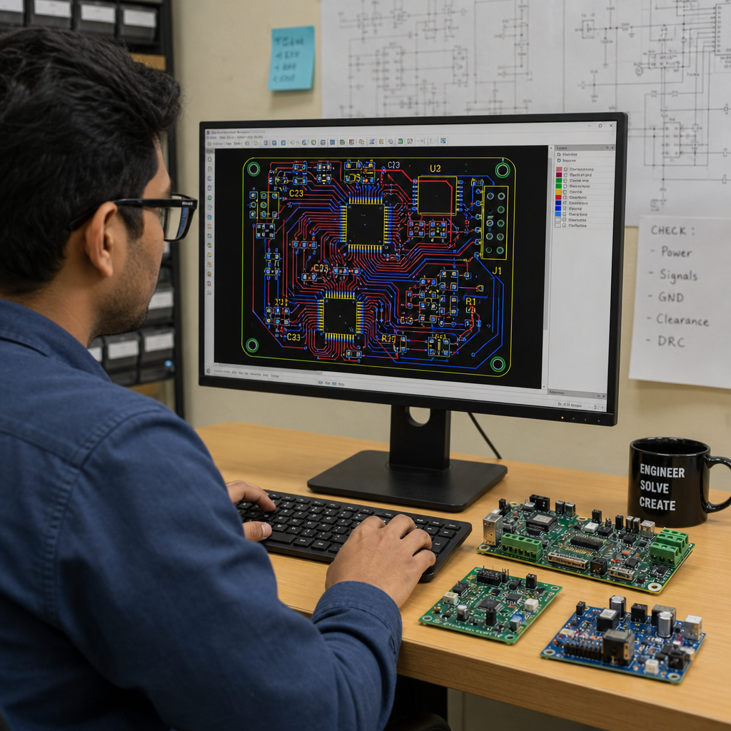
Understanding the Basics of Printed Circuit Board
A printed circuit board is the foundation that supports and connects electronic components inside many modern devices. From small LED products to industrial controls, the circuit board gives an electronic circuit a stable physical structure and a reliable path for electrical signals. Understanding the basics helps engineers, buyers, makers, and product teams make smarter decisions about circuit board design, pcb fabrication, pcb assembly, and printed circuit board testing.
What is a printed circuit board?
A printed circuit board, often shortened to PCB, is a flat board that mechanically supports electronic components and electrically connects them through patterned copper pathways. Instead of wiring every component by hand, manufacturers create a printed circuit pattern that routes power and signals between parts such as resistors, integrated circuits, connectors, a printed circuit board capacitor, fuses, LEDs, sensors, and switches.
The word “printed” can be slightly misleading. A PCB is not printed in the same way as a document from an office printer. In most cases, copper is laminated to an insulating base material, then selectively removed, plated, drilled, finished, and prepared so components can be attached. The result is a repeatable platform that allows complex electronics to be built in a compact and organized way.
For anyone developing custom pcbs, the printed circuit board is more than a support surface. It affects product size, signal quality, durability, heat behavior, assembly cost, inspection speed, repairability, and long-term reliability. A strong PCB plan can make a product easier to manufacture, while a weak design can create noise problems, overheating, solder defects, or failures in the field.

The basic structure of a circuit board
Most circuit boards are built from a combination of insulating material, copper, protective coatings, markings, and electronic components. The exact stack-up depends on the product, but the purpose is always the same: create stable electrical connections while keeping unwanted connections apart.
A simple board may have copper on one side only. More complex boards can use two, four, six, or many more layers to route dense signals and power networks. Layer count, material choice, copper thickness, and via style all influence pcb manufacturing cost, electrical performance, and production complexity.
The base material gives the board strength
The base material, often called the substrate, gives the board its shape and rigidity. Many standard boards use fiberglass-reinforced epoxy materials, while flexible circuits use bendable films and metal-core boards use a thermally conductive base. The right material depends on the environment, electrical needs, mechanical stress, and heat generated by the components.
A led printed circuit board, for example, may need better thermal performance than a simple low-power control board. LEDs can generate heat, and heat can reduce performance or shorten operating life if it is not managed. That is why LED boards often require careful material selection, copper planning, and mechanical design.
Copper traces create the electrical paths
Copper traces are the pathways that carry current and signals across the board. Their width, spacing, thickness, and route are determined during pcb design. A trace carrying a tiny signal does not need the same width as a trace feeding a motor, heater, or LED array.
Good trace planning helps reduce voltage drop, signal interference, and heat buildup. It also supports cleaner pcb fabrication because manufacturers need enough spacing to etch, plate, inspect, and finish the copper features accurately. When traces are too narrow or too close for the selected manufacturing process, the board may become harder to build consistently.
Solder mask protects the copper
The solder mask is the colored protective layer often seen on a finished circuit board. Green is common, but other colors may be used depending on preference, branding, inspection needs, or production standards. The solder mask helps prevent solder bridges, protects copper from oxidation, and reduces the chance of accidental electrical shorts.
Solder mask openings expose the pads where components will be soldered. The size and placement of these openings matter because they influence solder flow, inspection visibility, and assembly yield. Small details in the solder mask design can make a noticeable difference during pcb assembly.
Printed circuit board labels support identification
Printed circuit board labels and silkscreen markings help people identify components, polarity, connector orientation, test points, revision codes, and safety information. Clear labels make assembly, inspection, troubleshooting, and repair much easier. They also help reduce mistakes when a technician needs to confirm component position or board version.
Labels should be readable, placed where they will not be hidden by large components, and aligned with the way the board will be handled. In dense designs, it may not be possible to label everything on the board surface, so documentation and assembly drawings become especially important.
How does a circuit board move from idea to working product?
A circuit board moves from idea to working product through a structured process: requirements, schematic design, layout, fabrication, assembly, inspection, testing, and refinement. Each stage turns an electronic circuit from a concept into a physical board that can be manufactured, tested, and used reliably.
The process usually begins with a clear definition of what the board must do. Designers consider power input, operating environment, signal requirements, connectors, size limits, safety needs, and production volume. Those decisions guide the schematic, which shows how components connect electrically before anyone decides where parts will sit on the physical board.
A practical PCB development flow often includes:
- Define the requirements. Clarify voltage, current, functions, size limits, heat concerns, expected environment, and any regulatory or safety considerations.
- Create the schematic. Select parts and map the electronic circuit logically, including power rails, control signals, protection parts, connectors, and test points.
- Design the layout. Place components and route copper traces while considering electrical performance, manufacturability, thermal behavior, and assembly access.
- Review before release. Check design rules, footprints, polarity, clearances, component availability, and manufacturing notes before sending files out.
- Build prototypes. Use pcb fabrication and pcb assembly to create physical samples that can be inspected and tested.
- Test and revise. Perform functional checks, printed circuit board testing, and design updates before scaling production.
This flow is not only for large engineering teams. Makers, startups, product developers, and repair specialists can all benefit from the same disciplined approach. The earlier a problem is found, the easier and less expensive it usually is to fix.

Key parts commonly found on printed circuit boards
A finished PCB may hold only a few components or thousands of parts, depending on the product. Each component has a purpose within the circuit, and the board brings them together in a controlled layout. Knowing the common parts makes it easier to read a design, discuss requirements, and understand why placement matters.
Capacitors help stabilize and filter circuits
A printed circuit board capacitor stores and releases electrical energy in small amounts. Capacitors are often used for filtering noise, smoothing power, timing functions, and supporting integrated circuits during quick changes in current demand. They may look simple, but their placement can be critical.
For example, decoupling capacitors are often placed close to the power pins of integrated circuits. If they are too far away, they may not control noise effectively. In power sections, capacitor type, voltage rating, temperature rating, and layout can influence reliability and performance.
Fuses and fuse holders add protection
Printed circuit board fuses are used to help protect circuits from excessive current. If current rises beyond a selected limit, a fuse can open the circuit and reduce the risk of further damage. The right fuse choice depends on current rating, voltage, response time, operating temperature, and the type of fault the design must handle.
A printed circuit board fuse holder allows a fuse to be installed, removed, or replaced more easily. This can be useful in products where serviceability matters. Designers must leave enough space around the fuse holder for safe access, heat management, and mechanical stability.
Connectors, LEDs, and active components shape function
Connectors link the board to power sources, sensors, displays, batteries, cables, and other modules. Their position affects enclosure design, user access, cable routing, and mechanical stress. A connector placed without considering the final product can create assembly or service problems later.
LEDs may provide status indication, lighting, sensing, or display functions. In a led printed circuit board, thermal paths, current control, spacing, and optical alignment are important. Active components such as microcontrollers, drivers, memory chips, and communication devices often determine the board’s main intelligence and performance.
Practical circuit board design principles
Circuit board design is both technical and practical. A design must satisfy the schematic, but it must also be manufacturable, inspectable, and suitable for real-world use. Good layout work balances electrical requirements with production realities.
Designers often focus on component placement first because placement controls much of the routing quality. Power components, heat-generating parts, connectors, sensitive signals, and mechanical mounting points should be arranged intentionally. When placement is rushed, routing becomes harder and the board may need more layers or compromises.
Useful pcb design practices include:
- Keep power paths appropriate for the current. Wider traces, copper pours, and short routes can help manage higher current and reduce voltage drop.
- Separate noisy and sensitive areas. Switching power circuits, motors, radios, and precision analog signals may need careful spacing and grounding.
- Plan for heat early. Use copper area, thermal vias, material choices, and component spacing to help move heat away from critical parts.
- Use correct footprints. A footprint mismatch can cause assembly delays, weak solder joints, or unusable prototypes.
- Include test points. Accessible test points make debugging, production checks, and printed circuit board testing easier.
- Think about the enclosure. Mounting holes, connector locations, LED visibility, and keep-out zones should match the mechanical design.
- Respect manufacturing rules. Trace width, spacing, drill sizes, annular rings, solder mask clearances, and board edge requirements should fit the chosen process.
The best layouts are rarely accidental. They come from understanding how electricity behaves, how parts are assembled, and how the board will be used after it leaves the factory.
PCB fabrication turns design files into physical boards
PCB fabrication is the manufacturing stage that creates the bare board before components are attached. Fabricators use the design files to form copper patterns, drill holes, plate vias, apply solder mask, add silkscreen, and finish exposed metal surfaces. The result is a bare printed circuit board ready for assembly.
Newest in the store


Designers typically provide fabrication data such as copper layers, drill files, solder mask layers, silkscreen layers, board outline, and manufacturing notes. Clear documentation reduces back-and-forth questions and helps the fabricator understand special requirements. If the board needs controlled impedance, specific material, special thickness, or unusual finish, those details should be communicated early.
Custom pcbs support product-specific needs
Custom pcbs are designed for a specific function, size, enclosure, connector arrangement, or performance target. Unlike generic development boards, custom boards can be optimized for the final product. This can reduce wasted space, improve assembly efficiency, support branding, and create a cleaner user experience.
Customization also introduces responsibility. A custom design must be reviewed carefully because errors are built directly into the board. Footprint checks, design rule checks, schematic reviews, and prototype testing are essential steps before moving to larger production quantities.
PCB technology continues to evolve
PCB technology keeps expanding as products demand smaller size, faster signals, better thermal control, and more reliable manufacturing. Modern boards may include high-density interconnect features, flexible sections, rigid-flex construction, metal cores, advanced finishes, embedded passives, or materials suited for high-frequency use. Not every product needs advanced features, but knowing what is possible helps teams choose the right level of complexity.
A practical design approach avoids using advanced technology simply because it sounds impressive. The right board is the one that meets performance, reliability, manufacturability, and cost goals without unnecessary complexity. Simpler can be better when the application allows it.
PCB assembly adds the components
PCB assembly is the stage where electronic components are placed and soldered onto the fabricated board. Depending on the design, assembly may involve surface-mount components, through-hole components, or both. Surface-mount parts are common in compact electronics, while through-hole parts may be used for connectors, large components, fuses, or parts that need extra mechanical strength.
Assembly quality depends on many details: pad design, solder paste application, placement accuracy, soldering process, component orientation, and inspection. Even a well-designed board can fail if assembly instructions are unclear or if component data is incomplete. Clear bill of materials information, polarity markings, placement drawings, and special handling notes all support better outcomes.
Teams preparing for assembly should check:
- Whether every component footprint matches the selected part package.
- Whether polarized components have clear orientation markings.
- Whether tall, heavy, or heat-sensitive parts need special handling.
- Whether connectors and fuse holders can tolerate the selected soldering process.
- Whether printed circuit board labels remain visible after parts are installed.
- Whether inspection access is available for critical solder joints.
- Whether substitute components are acceptable if the preferred part is unavailable.
A thoughtful assembly plan helps prevent avoidable delays. It also makes troubleshooting easier because the board documentation matches the physical product.

Why does printed circuit board testing matter?
Printed circuit board testing matters because it helps confirm that the board was built correctly, performs as intended, and is safe to move into the next stage of use. Testing can catch open circuits, shorts, incorrect components, reversed parts, weak solder joints, functional problems, and design issues before the product reaches users.
Testing may happen at several points. Bare boards can be electrically checked before assembly. After assembly, boards may go through visual inspection, automated optical inspection, in-circuit checks, functional testing, programming, burn-in, or environmental evaluation depending on the product’s requirements.
A useful testing strategy should match the risk and complexity of the application. A simple indicator board may need basic continuity and function checks. A power control board, medical-related device, automotive module, or communication product may require more detailed validation, documentation, and process control.
Common goals of testing include:
- Confirming electrical continuity. The intended connections should exist, and unintended shorts should not.
- Verifying component placement. Parts must be installed in the right location and orientation.
- Checking function. The board should perform the required operations under expected conditions.
- Finding process issues. Repeated defects may reveal stencil, soldering, placement, or handling problems.
- Supporting traceability. Test records can help diagnose later failures and improve production control.
Testing is not a substitute for good design. It is a safety net and learning tool that helps turn prototypes into dependable products.
Common mistakes that make PCB projects harder
Many PCB problems are preventable. They often come from rushing early decisions, skipping reviews, or treating manufacturing as an afterthought. A little extra planning can save time once the board is in production.
One common mistake is choosing components before confirming availability, package type, and assembly suitability. A part may look correct electrically but be difficult to source, hard to solder, or unavailable in the chosen package. Another frequent problem is forgetting mechanical constraints such as enclosure walls, screw heads, cable bends, or connector access.
Watch for these issues before releasing a design:
- Missing or incorrect component footprints.
- Insufficient spacing around high-voltage, high-current, or heat-generating areas.
- Traces that are too narrow for the required current.
- Poorly placed capacitors that reduce filtering effectiveness.
- Fuse ratings that do not match the protection goal.
- Labels hidden under components or placed too close to pads.
- Test points that are inaccessible after assembly.
- Mounting holes that conflict with traces or components.
- No clear revision marking on the board.
- Incomplete fabrication or assembly documentation.
These checks are especially important for custom pcbs because the design is tailored to a specific product. If the board outline, connector placement, or mounting pattern is wrong, the issue may affect the entire product build.
Real-world uses of printed circuit boards
Printed circuit boards are used wherever electronics need a compact, repeatable, and organized structure. They appear in consumer devices, lighting products, industrial equipment, communication systems, power supplies, vehicles, appliances, security systems, test equipment, and many other applications. The board may be hidden inside a plastic enclosure, mounted in a metal cabinet, or exposed in a development kit.
In LED lighting, the board may support light output, current regulation, heat transfer, and connector placement. In a control system, it may connect sensors, relays, processors, and communication ports. In a battery-powered product, it may manage charging, protection, power conversion, and user indicators.
The variety of applications is one reason PCB knowledge is useful beyond engineering teams. Product managers, sourcing specialists, quality teams, technicians, and founders all make better decisions when they understand how board choices affect reliability, production, and service.
Staying current with printed circuit board news
Printed circuit board news can help teams stay aware of material trends, supply chain changes, manufacturing capabilities, design practices, and emerging pcb technology. While the basic purpose of a circuit board remains stable, the tools, materials, standards, and production methods around it continue to develop. Staying informed can help teams ask better questions and avoid outdated assumptions.
Useful sources of learning may include manufacturer application notes, fabrication guidelines, assembly house recommendations, engineering publications, standards organizations, webinars, and hands-on prototype reviews. For practical projects, the most valuable information often comes from combining technical reading with direct feedback from fabricators and assemblers.
When evaluating new information, focus on relevance. A high-speed telecommunications board, a simple LED driver, and a rugged industrial controller do not need the same design rules. Good judgment means applying the right lesson to the right product rather than copying advice without context.
A practical checklist before ordering boards
Before sending a design for pcb manufacturing, it helps to pause and review the essentials. This final check does not need to be complicated, but it should be systematic. The goal is to catch obvious issues while there is still time to fix them.
Use this pre-order checklist:
- Review the schematic against the product requirements.
- Run electrical rule checks and design rule checks.
- Confirm footprints against component datasheets and supplier information.
- Check current paths, fuse placement, and capacitor placement.
- Verify mounting holes, board outline, connector access, and enclosure fit.
- Make sure printed circuit board labels are readable and useful.
- Add test points for important power rails, signals, and programming lines.
- Confirm material, thickness, copper weight, solder mask color, and finish requirements.
- Review fabrication outputs before uploading or sending files.
- Prepare assembly files, bill of materials, polarity notes, and any special instructions.
- Plan how prototypes will be inspected, powered, programmed, and tested.
This checklist supports better communication with fabrication and assembly partners. It also creates a habit of reviewing the board as a physical product, not just as a layout on a screen.
The main takeaway
A printed circuit board is the organized platform that turns an electronic circuit into a manufacturable product. Its layers, copper routes, labels, components, fuses, capacitors, materials, and assembly details all influence how well the final device works.
For beginners, the best starting point is to understand the complete path: design the circuit, plan the layout, fabricate the bare board, assemble the components, and test the result. For experienced teams, the same fundamentals remain important because small layout and documentation choices can have a major effect on quality.
Whether you are exploring your first circuit board or preparing custom pcbs for production, a practical approach will serve you well. Keep the design clear, communicate requirements early, respect manufacturing limits, and make printed circuit board testing part of the plan from the beginning.