


The Evolution of circuit board Technology

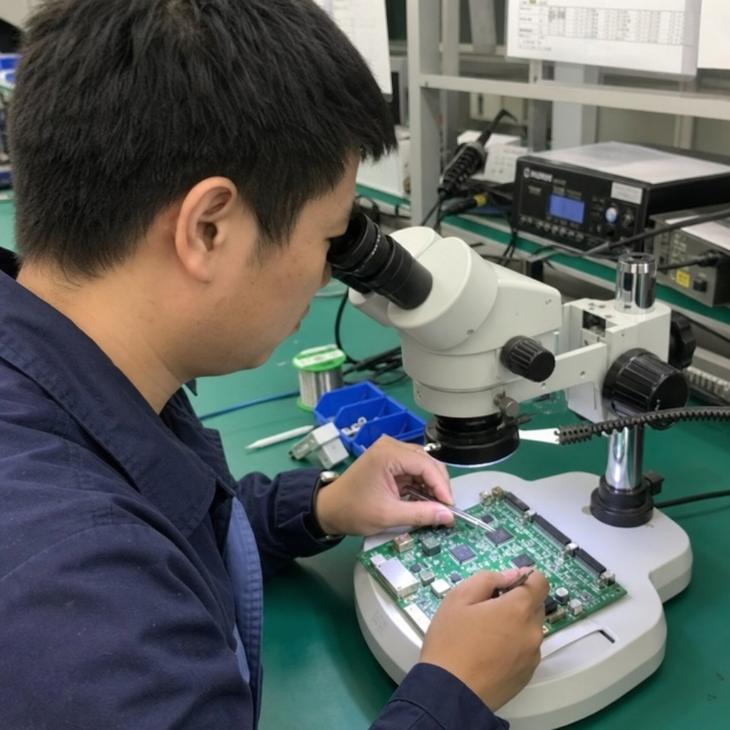
The Evolution of circuit board Technology
Circuit board technology has moved from simple hand-wired layouts to compact, multilayer platforms that power everything from household devices to advanced industrial systems. A modern printed circuit board is more than a support surface for parts; it is the foundation of an electronic circuit, influencing performance, reliability, heat control, repairability, and manufacturing efficiency. This article walks through how circuit board development has changed, what drives today’s pcb technology, and what designers, engineers, and buyers should understand when planning a new project.
How did circuit board technology evolve?
Circuit board technology evolved because electronics needed to become smaller, faster, more reliable, and easier to manufacture at scale. Early electronic devices relied on point-to-point wiring, where components were manually connected with individual wires. That approach worked for simple systems, but it became slow, bulky, and inconsistent as products grew more complex.
The printed circuit changed that pattern by replacing much of the manual wiring with conductive copper pathways on an insulating board. This made circuit fabrication more repeatable and allowed manufacturers to produce electronic assemblies with greater consistency. Over time, single-sided boards gave way to double-sided and multilayer boards, opening the door to denser circuit design and more capable devices.
Today, a printed circuit board can include fine traces, surface-mount components, controlled impedance routing, flexible materials, thermal management features, protective finishes, and clear printed circuit board labels. The result is a platform that supports modern electronics while helping teams control quality, production time, and long-term service needs.

From hand wiring to printed pathways
Before the printed circuit board became widely used, many electronic products were built with wires, terminal strips, and chassis-mounted parts. Technicians connected each element by hand, which required skill and patience. For low-volume equipment, this could be acceptable. For growing consumer, industrial, and computing markets, however, it created obvious problems.
Manual wiring introduced variation from one unit to another. A slightly different wire path could affect signal behavior, make repairs harder, or increase the risk of assembly mistakes. As products became smaller, there was also less room for loose wiring and bulky mechanical structures.
Printed pathways solved many of these issues. Copper traces could be etched or formed directly onto a substrate, creating consistent electrical routes between pcb components. This was a major step forward because the board itself became part of the product’s design logic. Instead of simply holding parts in place, the circuit board determined how power, signals, grounding, and mechanical layout worked together.
That shift still matters. Whether a project involves a compact sensor, a power controller, a led printed circuit board, or a communication module, the physical layout affects how the electronic circuit behaves. Good pcb design is not just about connecting points on a schematic. It is about arranging those connections so the finished product performs reliably in real operating conditions.
The rise of multilayer boards
Single-sided boards are useful for simple electronics, but they limit how many connections can fit in a small area. Double-sided boards improved density by placing copper on both sides of the substrate and using plated holes to connect layers. Multilayer boards extended that idea further by stacking internal copper layers between insulating materials.
This change transformed pcb technology. Designers could dedicate internal layers to power and ground planes, route complex signals more cleanly, and reduce board size without sacrificing function. In many modern products, multilayer construction is what makes compact design possible.
Multilayer boards also support better electrical performance when designed correctly. Ground planes can help manage return paths and reduce noise. Power planes can distribute current more evenly. Controlled layer stacks can help high-speed signals maintain more predictable behavior. These advantages are especially important in devices that handle data, wireless communication, motor control, imaging, or precision sensing.
However, multilayer pcb manufacturing also demands more planning. Layer count, material selection, via strategy, trace spacing, impedance requirements, and thermal behavior all affect cost and manufacturability. A design that looks efficient on screen may become expensive or difficult to build if fabrication limits are ignored. That is why strong communication between circuit design, layout, engineering, and manufacturing teams is essential from the beginning.
What makes modern pcb design different?
Modern pcb design is different because boards now need to satisfy electrical, mechanical, thermal, manufacturing, compliance, and service requirements at the same time. A circuit board is no longer treated as a flat carrier for components. It is a carefully engineered structure that must support performance across the full product lifecycle.
One major difference is density. Surface-mount technology allows smaller pcb components to be placed closer together, making products lighter and more compact. This creates more layout freedom, but it also increases the need for accurate spacing, solder pad design, inspection access, and heat planning.
Another difference is speed. Many electronic systems now move signals at frequencies where trace length, impedance, return path continuity, and crosstalk become serious concerns. In those cases, the printed circuit board is part of the signal path in a very literal sense. Poor routing can cause performance issues even when the schematic appears correct.
Thermal behavior is also more important. Power supplies, processors, LEDs, motor drivers, and charging circuits can generate significant heat. A led printed circuit board, for example, may need thoughtful copper distribution, thermal vias, metal-core materials, or heat-sink contact areas to protect brightness, efficiency, and operating life.
Finally, modern design must consider assembly and testing early. Pad shapes, part orientation, connector access, printed circuit board labels, and test points all influence pcb assembly quality. A board that is easy to build, inspect, and test is usually easier to scale.
Materials and fabrication keep expanding the possibilities
Traditional circuit boards often use rigid fiberglass-reinforced laminate, but the material landscape has broadened significantly. Different applications may call for rigid, flexible, rigid-flex, metal-core, high-temperature, high-frequency, or specialty substrates. Each material choice changes how the board handles heat, vibration, bending, moisture, and electrical behavior.
Rigid boards remain common because they are practical, cost-effective, and suitable for many products. Flexible boards are useful where space is tight or movement is required, such as wearable electronics, camera modules, medical devices, and compact consumer products. Rigid-flex boards combine stable component mounting areas with bendable interconnects, helping reduce connectors and cable assemblies.
Metal-core boards are often associated with LED and power applications because they can move heat away from components more effectively than many standard materials. A led printed circuit board may use this structure when thermal control is central to product performance. High-frequency materials, meanwhile, can help preserve signal quality in radio, radar, and high-speed communication designs.
Circuit fabrication methods have also improved. Modern processes can create finer traces, smaller holes, more consistent plating, cleaner solder masks, and more accurate registration between layers. These improvements do not eliminate design constraints, but they give engineers more tools for solving space and performance challenges.
Practical material considerations
When choosing a board material or fabrication approach, teams should consider more than the lowest unit cost. The right decision depends on the operating environment and product goals.
Useful questions include:
- Will the board face high heat, vibration, moisture, chemicals, or outdoor exposure?
- Does the circuit need controlled impedance or high-frequency performance?
- Are there high-current paths that require heavier copper or wider traces?
- Will the board bend during installation or during normal use?
- Does the enclosure limit board thickness, connector height, or heat dissipation?
- Can the selected material be sourced and manufactured consistently at the expected volume?
These questions help prevent a common problem: designing a board that works in an ideal prototype but struggles in actual use. Material selection is not just a technical detail. It is part of product reliability.
Components became smaller, smarter, and more specialized
The evolution of pcb components has shaped the evolution of the board itself. Through-hole parts once dominated because they were easier to handle and mechanically strong. They are still useful for connectors, large capacitors, power devices, fuses, and components that experience mechanical stress. But surface-mount components changed the economics and density of electronics.
Surface-mount parts reduce the need for drilled holes and allow components to be placed on one or both sides of the board. This supports automated pcb assembly and enables more compact layouts. Smaller packages also shorten electrical paths, which can benefit high-speed or low-noise designs when the layout is handled carefully.
Specialized components have also become more common. A printed circuit board capacitor may appear in many forms, from small decoupling capacitors near integrated circuits to larger bulk capacitors in power sections. Each type has a role. Decoupling capacitors help stabilize local supply voltage. Bulk capacitors support broader power demands. Placement, value, package size, voltage rating, and thermal conditions all matter.
Protection components are equally important. Printed circuit board fuses help protect circuits from excessive current. In some products, a printed circuit board fuse holder is used when a fuse may need to be replaced during maintenance. In other cases, resettable protection devices or soldered fuses may be more appropriate. The best choice depends on service expectations, available space, safety requirements, and the nature of the fault being protected against.
Clear labeling supports all of this. Printed circuit board labels, silkscreen markings, polarity indicators, reference designators, revision marks, and test point labels help assemblers, inspectors, and repair technicians understand the board quickly. Good labeling reduces confusion and can save time during debugging or field service.
PCB assembly turned boards into scalable products
A bare board becomes useful only when components are mounted, soldered, inspected, and tested. That is where pcb assembly plays a central role. Assembly connects the design vision to a physical product that can be shipped, installed, and used.
Modern assembly often combines automated solder paste printing, pick-and-place machines, reflow soldering, selective soldering, inspection, and functional testing. Automation improves speed and consistency, but it works best when the board has been designed with assembly in mind. Small layout decisions can create large production consequences.
For example, components that are placed too close together can make inspection difficult. Tall parts near small parts may interfere with automated placement or soldering. Connectors that lack mechanical support may fail under repeated use. Poorly oriented polarized components can increase the risk of assembly error if markings are unclear.Newest in the store


Design for assembly does not mean compromising performance. It means making the board easier to build correctly. A design that considers panelization, fiducials, solder mask clearances, component availability, placement access, and inspection points is usually more efficient to produce.
Assembly-friendly design habits
Practical habits that support smoother pcb assembly include:
- Use clear reference designators. Make printed circuit board labels readable and avoid placing them under components when possible.
- Keep component orientation consistent. Align similar parts in similar directions to simplify inspection and reduce mistakes.
- Provide useful test points. Add accessible points for power rails, ground, signals, and programming interfaces where testing is expected.
- Respect spacing rules. Leave enough room for soldering, inspection, heat flow, and rework.
- Confirm part availability early. A technically perfect footprint is not helpful if the part is unavailable or likely to change.
- Review mechanical fit. Check connectors, mounting holes, enclosure walls, cable paths, and service access before fabrication.
These habits are not glamorous, but they are powerful. They help reduce avoidable delays between prototype success and production readiness.

Testing moved from final check to design strategy
Printed circuit board testing used to be viewed mainly as a final production step. Today, effective teams think about testing much earlier. That shift is important because some faults are difficult or expensive to diagnose once a board is fully assembled inside a product.
Testing can include visual inspection, automated optical inspection, electrical continuity checks, in-circuit testing, boundary scan, programming verification, thermal evaluation, and functional testing. The right mix depends on the product, production volume, risk level, and complexity. A simple low-cost board may not need the same testing strategy as a safety-related industrial controller, but every board benefits from a plan.
Design choices can make testing easier or harder. Accessible test points allow faster measurement. Clear labels reduce interpretation errors. Sensible board partitioning can help isolate power, control, communication, and load sections. Good documentation helps technicians understand what they are seeing.
Testing also informs future improvements. If repeated faults appear in solder joints, component orientation, connector stress, or thermal hot spots, those findings should feed back into pcb design and pcb manufacturing decisions. In this way, testing is not just quality control. It is a learning system.
Reliability depends on the whole ecosystem
A reliable circuit board is not created by one decision. It results from alignment between circuit design, component selection, layout, fabrication, assembly, testing, and operating environment. Weakness in any one area can affect the whole product.
For example, a power section may use suitable components but fail if copper traces are too narrow for the current. A communication circuit may use the correct integrated circuit but suffer from poor grounding or noisy routing. A board may pass electrical tests but fail in the field if connectors experience mechanical stress or if heat has nowhere to go.
This is why experienced teams evaluate boards as systems. They consider how pcb components interact electrically and physically. They review how the enclosure affects airflow and heat. They check whether printed circuit board fuses are accessible if the product is designed for service. They confirm that printed circuit board labels remain readable after assembly.
Reliability also depends on documentation. Revision control, bill of materials accuracy, assembly drawings, testing notes, and fabrication files all help prevent confusion. When changes are made, the board record should make those changes visible. This is especially important when a product has multiple versions or when replacement boards must remain compatible with existing systems.
Sustainability and repairability are gaining attention
As electronics appear in more products, businesses and designers are paying closer attention to waste, repairability, and responsible manufacturing. A printed circuit board contains materials, components, and processing effort that should not be treated casually. Better design choices can support longer product life and more practical maintenance.
Repairability starts with access. If a fuse is expected to be replaced, a printed circuit board fuse holder may make sense. If connectors or switches are likely to experience wear, they should be placed where service is realistic. Clear markings, logical layout, and available documentation can help technicians diagnose issues instead of replacing entire assemblies unnecessarily.
Sustainability can also be supported by right-sizing the design. Overly complex boards may consume more material and create more failure points than needed. On the other hand, under-designed boards may fail early and lead to more waste. The goal is balance: enough robustness for the application, without unnecessary complexity.
Component selection plays a role as well. Parts with stable supply chains, suitable ratings, and realistic lifecycles reduce redesign pressure. When a critical component becomes unavailable, teams may be forced to revise the layout, repeat printed circuit board testing, and update assembly processes. Designing with lifecycle awareness can reduce disruption.
Printed circuit board news reflects a fast-moving industry
Anyone following printed circuit board news will notice recurring themes: miniaturization, supply chain resilience, automation, advanced materials, high-speed design, power density, and more attention to environmental impact. These themes are connected. As products become smaller and more capable, boards must handle more work in less space while remaining manufacturable and reliable.
One practical takeaway is that pcb technology does not evolve in isolation. It responds to pressure from product design, manufacturing capability, component availability, end-user expectations, and service requirements. A board for an LED lighting product faces different priorities than a board for a wearable device, an industrial controller, or a communications module.
Keeping up with industry developments can help teams avoid outdated assumptions. For instance, newer fabrication options may make a compact layout possible, but they may also require tighter documentation and more careful cost planning. More advanced components may improve performance, but they can introduce new layout, testing, or thermal challenges.
The best approach is not to chase every new method. It is to understand which developments actually solve the problem in front of you.
Practical guidance for better board projects
Whether you are planning a new product, updating an existing electronic circuit, or reviewing a supplier’s proposal, it helps to approach the circuit board as a complete system. The following checklist can guide more practical decisions.
Project planning checklist
- Define the operating environment. Identify temperature range, vibration, moisture, electrical noise, and mechanical stress.
- Clarify electrical priorities. Know which signals are sensitive, which paths carry high current, and which sections generate heat.
- Plan component placement early. Put connectors, controls, displays, sensors, fuses, capacitors, and heat-generating parts where they make practical sense.
- Think about manufacturing limits. Confirm trace widths, spacing, drill sizes, layer count, finish options, and tolerances before finalizing the layout.
- Design for assembly. Make pcb assembly easier with clear markings, consistent orientations, good spacing, and accessible inspection areas.
- Design for testing. Add test points and labels where they will help production checks, troubleshooting, and firmware programming.
- Review service needs. Decide whether printed circuit board fuses, connectors, or other replaceable parts need user or technician access.
- Control documentation. Keep schematics, layout files, bills of materials, assembly drawings, and test procedures aligned.
This checklist is simple, but it prevents many avoidable problems. It encourages teams to think beyond the layout screen and consider the real journey from concept to finished product.
Common mistakes that slow down pcb manufacturing
Many board issues are not caused by a lack of creativity. They are caused by skipped details. A layout can look complete and still create problems during pcb manufacturing if it ignores fabrication or assembly realities.
A common mistake is treating the board outline as an afterthought. Mounting holes, connector locations, edge clearances, and enclosure constraints should be confirmed early. If the mechanical fit is wrong, even a well-designed printed circuit can become unusable.
Another mistake is placing components without considering heat. A printed circuit board capacitor located too close to a hot component may experience unnecessary stress. Power components that lack enough copper area or airflow may run hotter than expected. LED designs can suffer if heat is trapped near the light source.
Teams also run into trouble when they leave testing until the end. Without accessible test points, troubleshooting becomes slower. Without clear printed circuit board labels, technicians may spend extra time identifying parts and signals. Without documented acceptance criteria, production teams may not know whether a board truly passes.
Finally, some projects underestimate the importance of supplier communication. Fabricators and assemblers need complete, consistent files. If the design data, bill of materials, solder paste layer, drill files, and assembly notes do not match, delays are likely.
The future is smarter, denser, and more connected
The future of circuit board technology will likely continue in the same broad direction: more capability in smaller spaces, stronger integration between design and manufacturing, and greater attention to reliability across the product lifecycle. Boards will keep adapting to high-speed communication, power conversion, sensing, automation, lighting, mobility, and connected devices.
Design tools will continue to help engineers simulate, check, and validate layouts before production. Manufacturing systems will continue to improve precision and repeatability. Testing will become more integrated into the design process, not just added at the end. These changes can make electronics more capable, but they also raise expectations for careful planning.
For businesses, the most practical lesson is clear: do not treat the circuit board as a commodity part too early. Even when a board is small or inexpensive, it carries the logic, power, and reliability of the product. Better decisions in pcb design, circuit fabrication, pcb assembly, and printed circuit board testing can reduce risk and make scaling easier.
Circuit board technology has come a long way from hand-wired electronics, and its evolution is still shaping how modern products are built. The strongest results come from balancing innovation with practical engineering: choose the right materials, place components thoughtfully, design for manufacturing, label and test clearly, and keep the full product environment in mind. A well-planned printed circuit board does more than connect components; it supports a product that works reliably, can be manufactured efficiently, and is easier to maintain over time.