


INA333 Instrumentation Amplifier: 7 Checks Before Raising Gain

INA333 Instrumentation Amplifier: 7 Checks Before Raising Gain
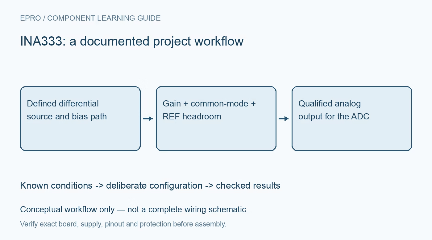
Plan an INA333 signal chain around differential gain, common-mode headroom, a low-impedance REF source and input bias paths before accepting an amplified signal. This is a documentation-based planning guide, not a report of independent hands-on testing.
1. Define the amplifier’s role in the signal chain
The INA333 is an analog instrumentation amplifier, not a digital sensor or a complete calibrated measurement system. Identify the differential source, expected common-mode voltage, bandwidth and downstream ADC before choosing gain. Record the exact supply arrangement and schematic rather than treating a breakout board as a universal interface. A related current-sense amplifier may illustrate output headroom, but its input architecture and allowable operating conditions are not interchangeable with those of this instrumentation amplifier. Manufacturer documentation.
2. Choose gain from the complete signal envelope
A single external resistor establishes gain using G = 1 + 100000/RG when RG is expressed in ohms. Include resistor tolerance, sensor offset and the largest expected differential signal in the calculation. Raising gain also amplifies unwanted differential offset and can consume the available output swing before the useful signal reaches its maximum. Leave justified margin for temperature, component variation and transient conditions. Do not infer a valid design from the nominal sensor amplitude alone. Manufacturer documentation.
3. Check common-mode and output constraints together
Input common-mode range depends on supply voltage and the amplifier’s internal and output operating points. The rail-to-rail output description does not mean every input combination remains linear right up to either supply. Use the manufacturer common-mode-versus-output guidance for the chosen gain and supply. Some overload conditions can produce an output that appears ordinary rather than obviously clipped. Check input voltages directly during validation instead of accepting a near-zero output as proof that neither input is overloaded. Manufacturer documentation.
4. Drive REF from a suitable low-impedance source
The output is referred to the REF pin, so a deliberate reference voltage can position a bipolar differential signal within a single-supply ADC range. That reference must remain low impedance to preserve common-mode rejection. An unbuffered divider may not meet the requirement just because its unloaded midpoint is correct. Evaluate the reference source under operating conditions and during startup. Include its noise, tolerance and available headroom in the output-error budget rather than treating REF as an ideal software offset. Manufacturer documentation.
Newest in the store




5. Provide a return path for input bias current
Both amplifier inputs require a defined DC path for their bias currents. A floating sensor, transformer or capacitively coupled source can otherwise drift outside the valid common-mode region. Use a return arrangement appropriate to the source and analyze the resistance balance and resulting offset. The small bias-current specification does not remove this requirement. Document the return path on the schematic, including what happens when the sensor cable is disconnected, rather than relying on incidental leakage through test equipment. Manufacturer documentation.
6. Match filtering and ADC loading to the application
Choose bandwidth and filtering using the actual signal and interference environment. Review input-filter matching so common-mode interference is not inadvertently converted into differential error. At the output, check the ADC’s acquisition behavior, capacitive loading and reference range rather than assuming that a slow display rate means the analog load is gentle. Provide the documented local supply bypassing. Treat amplifier settling, ADC settling and digital averaging as separate parts of the response-time and noise analysis. Manufacturer documentation.
7. Validate gain without hiding saturation in calibration
Begin with known safe differential inputs at several common-mode levels inside the approved region. Compare the expected gain and reference offset with the measured output, then check the downstream conversion independently. Include startup, a disconnected source and representative signal extremes. Save supply, REF, input and output voltages with the resistor value and test conditions. A calibration offset cannot repair clipping or an invalid bias path, so establish linear operation before fitting a correction factor. Manufacturer documentation.
Related reading: INA180 Current Amplifier: 7 Checks Before ADC Readings.
Catalog note: The exact-part search did not return a matching Epro listing during preparation. Check the current catalog; this guide makes no price, availability or included-accessory claim.