


TMUX1101 Analog Switch: 7 Checks for a High-Impedance Signal

TMUX1101 Analog Switch: 7 Checks for a High-Impedance Signal
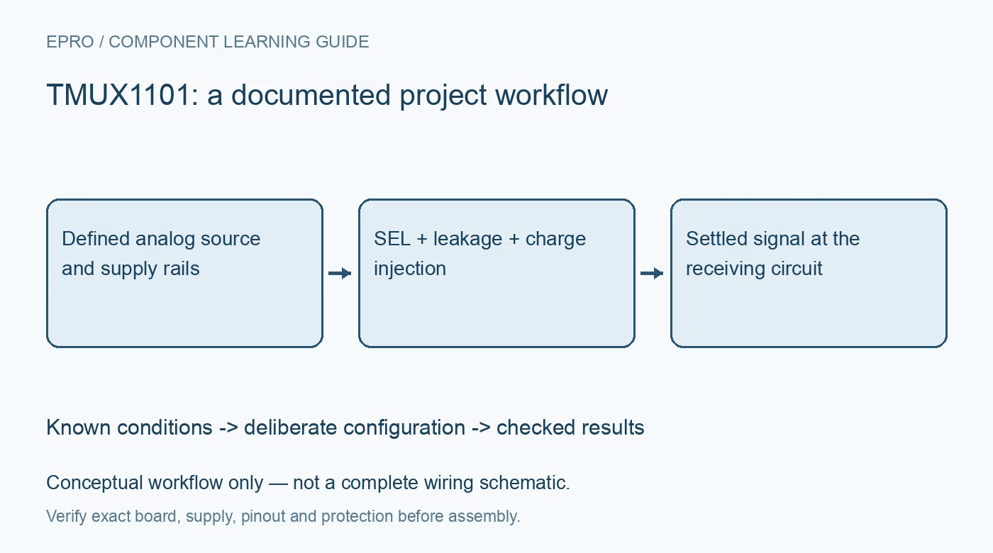
Plan a TMUX1101 signal path around rail limits, select polarity, leakage, charge injection and settling without confusing fail-safe logic with analog isolation. This is a documentation-based planning guide, not a report of independent hands-on testing.
1. Confirm the switch and its select polarity
The TMUX1101 is a single-pole, single-throw switch that conducts when SEL is high. Its TMUX1102 relative uses the opposite control polarity. Confirm the complete part number, package pinout and board wiring before assigning an enabled state in firmware. The signal path is bidirectional, but bidirectional conduction is not automatic voltage translation. Identify the source, receiver and intended disconnected condition rather than copying a digital bus-buffer schematic into an analog switching application. Manufacturer documentation.
2. Keep the analog signal inside the powered rails
The documented signal range extends from ground to VDD during normal operation. Check both switch terminals for expected DC levels, transients and conditions when one attached circuit remains powered independently. A small differential voltage across the closed switch does not establish that either terminal is within its allowed range. Include startup and shutdown in the review. Do not assume that an open switch provides galvanic isolation or that it can safely separate arbitrary positive and negative voltages. Manufacturer documentation.
3. Apply fail-safe logic to the control pin only
The fail-safe logic feature allows the SEL pin to be driven under documented conditions even when the switch supply is absent. That is a control-input feature, not a blanket guarantee of powered-off protection for the analog terminals. Review those terminals separately using their actual limits and external circuitry. Choose a defined default for SEL during host reset. A safe digital control level does not automatically make an independently powered sensor or charged capacitor safe to connect to the signal path. Manufacturer documentation.
4. Budget leakage using the real environment
Very low typical leakage is attractive for high-impedance measurements, but temperature, signal level and board cleanliness matter. Compare the applicable limits with source impedance and the allowed voltage error. Flux residue, connectors, protective components and a test probe can dominate the integrated switch’s contribution. Document the complete leakage path rather than quoting one room-temperature typical number as a system guarantee. Include the disconnected state and the receiver’s own input current when evaluating whether a node remains at its intended voltage. Manufacturer documentation.
Newest in the store


5. Treat on-resistance as a circuit element
The closed switch adds resistance that depends on operating conditions. Evaluate its effect with the source resistance, receiver load, filtering and current through the path. A low nominal resistance does not imply zero gain error or zero distortion in every arrangement. Check both signal directions where the application uses them. Keep a load-current budget as well as a voltage-range budget; a precision signal switch is not automatically a suitable load-power switch simply because a continuity test shows conduction. Manufacturer documentation.
6. Allow switching transients to settle
Changing SEL injects charge and couples control activity into the analog path. A high-impedance node with small capacitance can show a noticeable voltage step even when the average leakage is tiny. Review charge injection, capacitance, source impedance and the receiving ADC’s acquisition behavior together. Define a settling interval after selection and before accepting a sample. Digital acknowledgement of the control command is not evidence that the analog node has recovered to the required accuracy. Manufacturer documentation.
7. Qualify connected and disconnected measurements
Compare the final circuit with the switch on and off under bounded signal conditions. Record source voltage, supply, select timing, receiver behavior and relevant temperature. Include repeated switching, a long disconnected interval and host reset in the evaluation. Separate a real source change from switching artifacts and retained capacitor charge. The qualification should establish a usable measurement window for that assembly, without claiming perfect isolation, universally negligible leakage or an unmeasured transient performance from datasheet typical values alone. Manufacturer documentation.
Related reading: TCA9803 I2C Buffer: 7 Checks Before Adding Pull-Ups.
Catalog note: The exact-part search did not return a matching Epro listing during preparation. Check the current catalog; this guide makes no price, availability or included-accessory claim.