


ADS8326 SAR ADC: 7 Checks for Clocked Acquisition and Unsigned Codes

ADS8326 SAR ADC: 7 Checks for Clocked Acquisition and Unsigned Codes
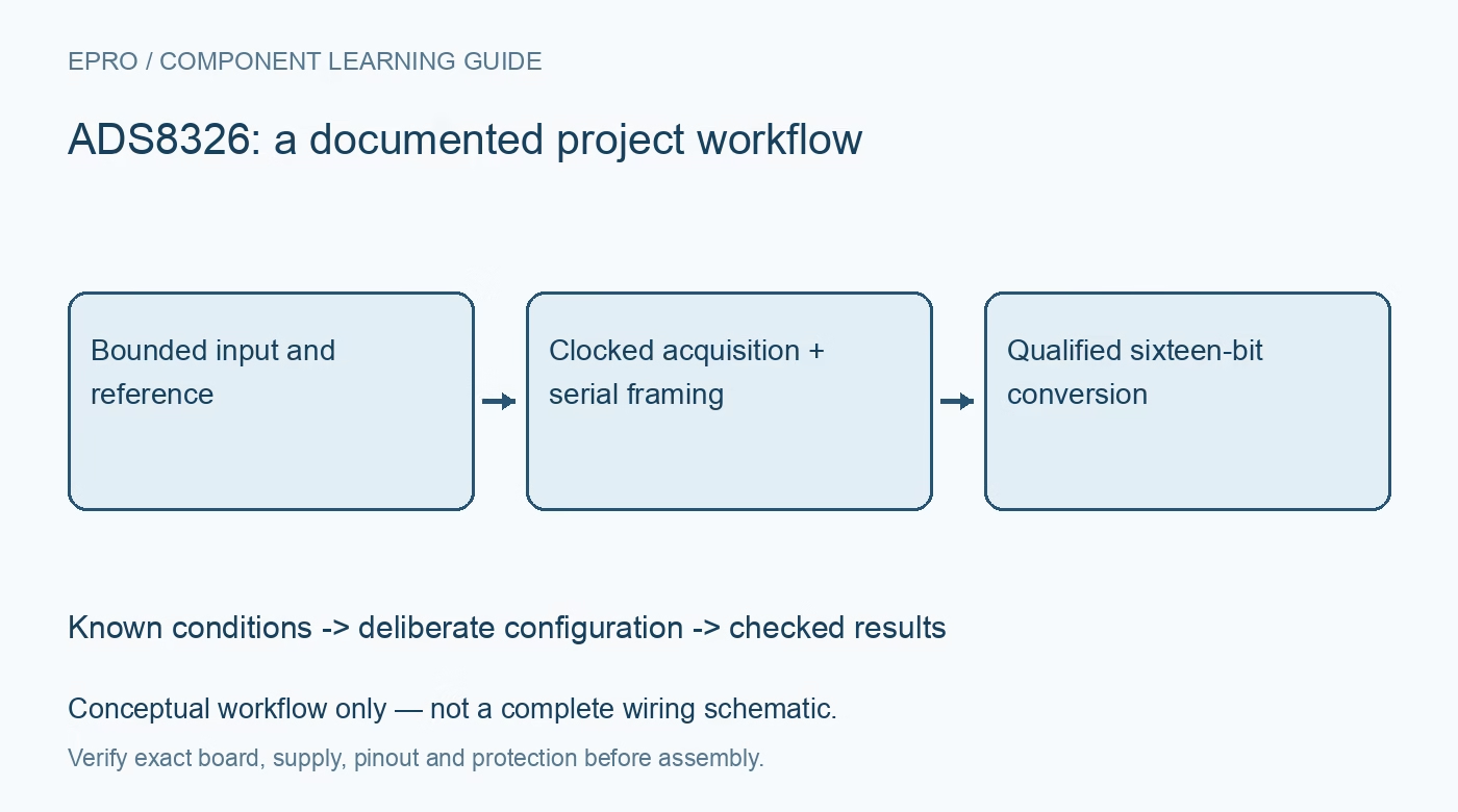
Check ADS8326 clock-dependent acquisition, near-ground negative input, reference range and straight-binary framing before interpreting sample voltage. This is a documentation-based planning guide, not a report of independent hands-on testing.
1. Identify the clock-driven conversion architecture
ADS8326 is a sixteen-bit SAR converter with a synchronous serial interface, an external reference and an external clock. Its acquisition and conversion behavior must be planned together with the host transfer rather than borrowed from an ADC with a separate independent conversion-start scheme. Confirm the actual package and board schematic before using a driver. Record supply, reference, sample rate, clock and input arrangement. A broadly SPI-compatible label describes an interface family, not every detail of a valid transaction. Manufacturer documentation.
2. Keep the negative input within its limited range
The converter measures the difference between plus-IN and minus-IN, but minus-IN is constrained near ground in normal operation. The datasheet specifies its allowed range and the relationship between the positive input and reference span. This is not a general-purpose fully differential bipolar interface. Check each input relative to ground as well as the differential voltage. For initial qualification, use a bounded source with a defined return, and do not connect a floating sensor merely because two analog input pins are present. Manufacturer documentation.
3. Choose the reference with realistic resolution expectations
The documented reference range extends from 0.1 V to VDD, but reducing reference voltage also reduces code size and increases the importance of noise and other errors relative to full scale. Evaluate the reference driver, its dynamic load and local decoupling at the intended conversion rate. Do not assume that a smaller span automatically produces a more accurate instrument. Keep reference uncertainty, ADC offset, gain error and source error distinct in the final voltage budget and use the applicable supply-condition specifications. Manufacturer documentation.
4. Let acquisition requirements constrain the serial clock
The analog source charges an internal sampling network during a defined number of clock cycles. Raising the clock rate shortens the available settling interval, so clock selection is also an analog-design choice. Use the manufacturer timing and drive guidance for the actual supply voltage and source impedance. A divider that appears fine with a slow test transfer may fail when production firmware raises the SPI clock. Qualify the intended fastest acquisition pattern, including channel or stimulus changes if applicable. Manufacturer documentation.
Newest in the store




5. Verify chip-select, leading bits and data alignment
Follow the serial timing diagram for chip-select assertion, acquisition, conversion and output-bit placement. Confirm which edge the host samples and where the first valid data bit appears in the received buffer. Padding or dummy clocks must not be silently interpreted as conversion bits. Capture a representative transaction if timing is uncertain and compare it against known codes. Avoid replacing the documented frame with a guessed two-byte read just because the converter resolution happens to be sixteen bits. Manufacturer documentation.
6. Apply the unipolar straight-binary transfer function
The data is straight binary, with zero, midscale and full-scale codes corresponding to the documented unipolar input span. The most significant bit is not a negative sign. Verify software scaling with synthetic codes and preserve the selected reference and input-return convention in the calculation. No pipeline delay does not mean the result arrives before conversion or that an unsettled source is corrected automatically. Keep raw codes and flag saturation rather than reporting an apparently precise voltage beyond the supported range. Manufacturer documentation.
7. Recheck burst operation and power-related transitions
The converter’s low-power operation depends on the acquisition schedule and time spent inactive. Check the documented clock-rate and power behavior rather than stretching a transaction indefinitely to save power. Compare stable-input results during continuous sampling and the actual burst schedule after allowing the required reference and input recovery. Record supply voltage, clock timing, reference, source impedance and frame extraction. This guide defines a documentation-based verification plan, not a bench characterization, and does not establish accuracy from resolution or low average power alone. Manufacturer documentation.
Related reading: ADS1262 Precision ADC: 7 Checks Before Trusting 32-Bit Data.
Catalog note: The exact-part search did not return a matching Epro listing during preparation. Check the current catalog; this guide makes no price, availability or included-accessory claim.