


INA826 Instrumentation Amplifier: 7 Checks for REF and Gain Headroom

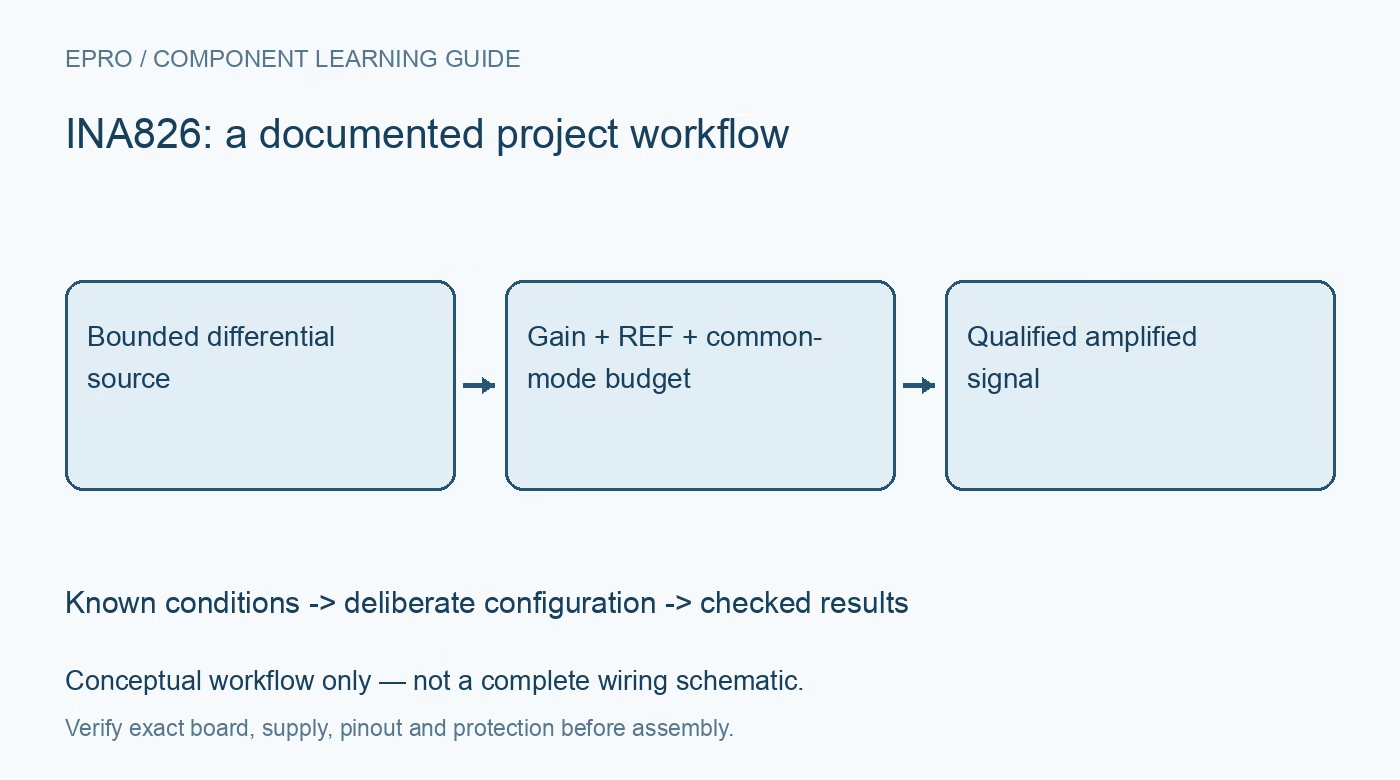
INA826 Instrumentation Amplifier: 7 Checks for REF and Gain Headroom
Design an INA826 signal path with the correct gain resistor, low-impedance REF drive, input bias return and common-mode versus output headroom. This is a documentation-based planning guide, not a report of independent hands-on testing.
1. Define the differential source and supply arrangement
INA826 is an instrumentation amplifier with gain set by one external resistor. Confirm the complete part, package, supply arrangement and actual signal source before selecting gain. Identify both input voltages relative to the amplifier supplies, not only their small difference. A low differential signal can sit at an unsuitable common-mode voltage. Document the expected input span, source impedance, offset and transients so later calculations represent the real sensor rather than an idealized bridge or a convenient test generator. Manufacturer documentation.
2. Use the INA826 gain equation rather than a related part’s
The nominal gain relationship is one plus 49.4 kilohms divided by the external gain resistor, with the documented unity-gain arrangement when that resistor is omitted. Do not reuse the gain constant from another instrumentation amplifier merely because its package or name looks similar. Include resistor tolerance and drift in the error budget. Check the actual fitted component and expected output demand before applying the final sensor, and distinguish nominal gain from guaranteed complete-system accuracy across temperature. Manufacturer documentation.
3. Check the coupled input and output operating region
The valid input common-mode range depends on gain, differential input, output demand and reference voltage. Consult the applicable operating-region curves rather than combining independent rail-to-rail assumptions. Internal amplifier nodes can constrain operation even when each external pin seems close to a permitted rail. Evaluate both ends of the sensor span and relevant offset conditions. A plausible output at one point does not establish linear operation over the full measurement range or during startup and recovery from a large input. Manufacturer documentation.
4. Drive REF from a suitably low impedance
The output is developed relative to the REF pin, which can establish a useful output offset for a single-supply acquisition chain. The manufacturer recommends a very low source impedance because added REF impedance degrades the internal resistor balance and common-mode rejection. A bare high-value divider is not automatically an adequate reference driver. Use the appropriate buffered or low-impedance arrangement and include its error and settling in the budget. REF changes the output reference; it does not remove input-stage common-mode constraints. Manufacturer documentation.
Newest in the store


5. Provide a DC return for input bias currents
Every input needs an appropriate bias-current return path. Floating sensors, transformers or AC-coupled signals can otherwise leave the amplifier without a valid operating point even if the differential signal is small. Follow the manufacturer examples for the source topology and consider the balance of source impedances. Keep leakage, contamination and protection components in the review. A rail-clipped output may indicate a missing return or common-mode violation rather than an unexpectedly large physical quantity at the sensor. Manufacturer documentation.
6. Budget bandwidth, filtering and ADC acquisition
Bandwidth changes with gain, and the complete chain includes source filtering, amplifier dynamics, output loading and the ADC’s acquisition behavior. Choose filter components with attention to matching and their effect on common-mode rejection. Check settling at the intended sample schedule instead of relying on the unity-gain headline bandwidth. Observe representative input steps within safe limits and allow appropriate recovery after power or configuration changes. Extra averaging cannot repair a systematic error caused by an unsettled or saturated analog path. Manufacturer documentation.
7. Validate differential scaling and common-mode rejection separately
Apply known bounded differential inputs at several relevant common-mode levels and compare against suitable reference measurements. Record supplies, gain resistor, REF source, input-return network, load, ADC settings and temperature conditions. Preserve raw readings and flag clipping rather than extrapolating through an invalid region. Input-protection ratings do not extend the normal measurement range. This manufacturer-based checklist does not claim independent amplifier characterization; recheck the coupled headroom and settling whenever gain, supply, reference driver or sensor connection changes. Manufacturer documentation.
Related reading: INA333 Instrumentation Amplifier: 7 Checks Before Raising Gain.
Catalog note: The exact-part search did not return a matching Epro listing during preparation. Check the current catalog; this guide makes no price, availability or included-accessory claim.