


SN74LVC1G17 Buffer: 7 Checks for Noninverting Schmitt Conditioning

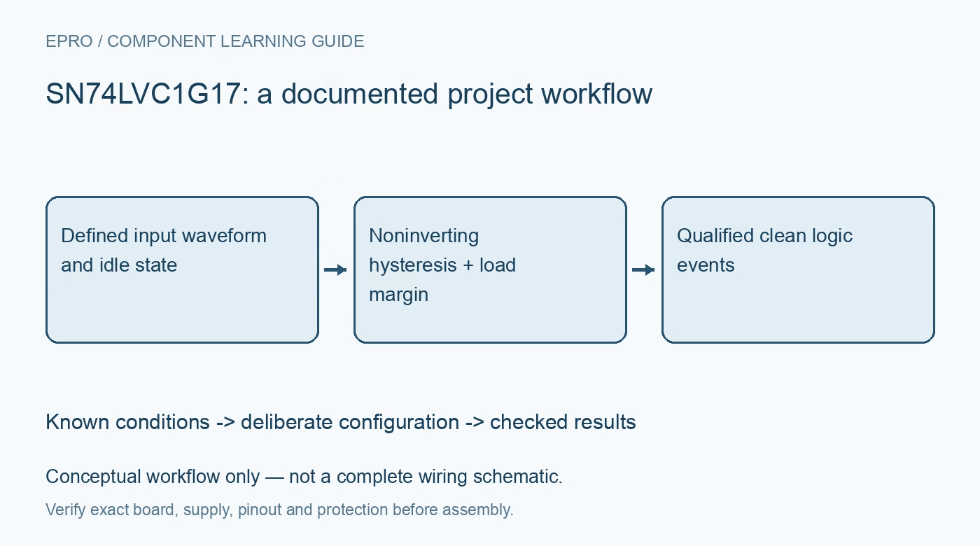
SN74LVC1G17 Buffer: 7 Checks for Noninverting Schmitt Conditioning
SN74LVC1G17 checks for preserved polarity, hysteresis limits, down-translation, powered-off behavior and event qualification. This is a documentation-based planning guide, not a report of independent hands-on testing.
1. Preserve polarity with the correct logic function
The SN74LVC1G17 is a single noninverting Schmitt-trigger buffer: the Boolean function is Y equals A. It is not the inverter function provided by similarly named Schmitt gates, and it has no general output-enable input. Confirm the exact package pinout before routing a small board or replacing another device. Preserved logic polarity can simplify an active-high enable or event signal, but the buffer is not a separate safety interlock and cannot determine whether the incoming command itself is valid. Manufacturer documentation.
2. Match supply and translation direction
The recommended supply range is 1.65 V to 5.5 V, and inputs accept up to 5.5 V within their specified conditions. This permits down-translation from a 5 V-domain signal when the buffer is supplied at 3.3 V. The output remains associated with its own supply; powering it at 3.3 V does not create a 5 V output. Check input thresholds, output loading and the receiving device’s requirements separately rather than describing the part as a universal bidirectional level converter. Manufacturer documentation.
3. Analyze both Schmitt thresholds
The positive-going and negative-going input thresholds differ, creating hysteresis that reduces repeated switching around a single boundary. The thresholds and hysteresis are supply-dependent quantities with specified limits, not a precision reference fixed at half VCC. Compare the expected signal and noise envelope with the complete threshold bands. A slow input can be converted into a clean output edge, but the exact analog crossing time varies. Do not use a logic buffer as an accurately calibrated voltage detector without an appropriate error analysis. Manufacturer documentation.
4. Separate edge conditioning from event qualification
A contact, cable or noisy sensor can cross both Schmitt thresholds repeatedly, producing several valid output transitions. One buffer therefore does not guarantee one pulse per button press or eliminate every glitch. Define the required minimum event duration and acceptable delay before selecting an RC network or software qualification. Include component tolerances, input leakage and threshold limits in that calculation. Verify representative disturbances rather than promising that a particular capacitor value debounces all possible switches or input sources. Manufacturer documentation.
Newest in the store


5. Review partial-power-down paths throughout the board
The Ioff feature supports specified partial-power-down operation and limits damaging backflow through the device when VCC is zero. It does not remove all current paths through a connected sensor, host, pull-up or protection component. Check the permitted input and output voltages under the actual sequencing conditions and include any externally held output. A powered-off logic pin that appears high-impedance is not galvanic isolation. Test benign low-voltage power transitions before relying on the buffer to separate independently powered subsystems. Manufacturer documentation.
6. Evaluate the real output load and decoupling
The propagation-delay and output-drive figures apply to documented supplies and loads. The headline maximum delay at 3.3 V is not a timing guarantee for an arbitrary long cable or large capacitor. Provide suitable local decoupling and a short return path, then check high and low output voltages at the receiving load. Do not use the logic output as a motor or lamp power switch. Package choice also affects layout feasibility; a very small footprint requires assembly and probing methods appropriate to its pin spacing. Manufacturer documentation.
7. Count accepted events at the final receiver
Record supply, input levels, threshold assumptions, load, output polarity and the number of detected events. Exercise slow ramps, expected noise, the intended contact action and power sequencing. Verify the downstream controller’s behavior rather than judging only the edge appearance on an oscilloscope. Preserve the distinction between clean transitions and valid application events. The resulting qualification should show correct noninverting conditioning while leaving surge protection, precise threshold measurement and application-specific glitch rejection as separate requirements that must also be addressed. Manufacturer documentation.
Related reading: SN74LVC2G14 Schmitt Inverter: 7 Checks for Clean Logic Edges.
Catalog note: The exact-part search did not return a matching Epro listing during preparation. Check the current catalog; this guide makes no price, availability or included-accessory claim.