


OPA391 Precision Buffer: 7 Checks for Low Bias and Real Error Limits

OPA391 Precision Buffer: 7 Checks for Low Bias and Real Error Limits
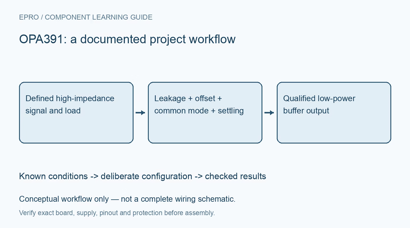
OPA391 checks for package-specific offset, common-mode effects, leakage control, capacitive loading and low-power settling. This is a documentation-based planning guide, not a report of independent hands-on testing.
1. Identify the channel and package specification
The OPA391 is the single-channel member of the OPAx391 family, with dual and quad relatives documented alongside it. Electrical tables and availability can differ by package, so retain the full ordering code rather than applying every family headline to every device. The supply range is 1.7 V to 5.5 V. Its low quiescent current and rail-to-rail description are useful starting points, but neither establishes input accuracy or output swing under the actual source, load and temperature conditions. Manufacturer documentation.
2. Separate typical bias from guaranteed error
The 10 femtoamp input-bias headline is a typical room-temperature figure, not a universal maximum through temperature and production variation. Use the table corresponding to the selected package and relevant temperature range. Multiply bias current by source impedance when estimating its contribution to input error, then include input offset, noise and reference errors separately. A high-impedance sensor can be limited more by board leakage than the amplifier itself, so very small typical bias should not become an unsupported system-level accuracy claim. Manufacturer documentation.
3. Check common-mode dependence of offset
For the OPA391DCK table, the familiar maximum 45 microvolt offset applies under specified conditions. A separate entry near the positive rail, at VCM equal to V+ minus 0.3 V with the stated supply, allows a much larger maximum offset of 750 microvolts. Rail-to-rail input range therefore does not mean constant precision throughout that range. Review the operating common-mode voltage as well as signal amplitude, and use the applicable error limit instead of extending a mid-supply specification to every input position. Manufacturer documentation.
4. Design the board for the source impedance
Leakage through contamination, connectors, humid surfaces, protection parts and test equipment can exceed the amplifier’s very low input-bias contribution. Choose cleaning, layout, insulation and any guarding approach appropriate to the source impedance and environment. Check resistor-network noise and leakage rather than optimizing only nominal resistor ratios. A handheld meter or probe can itself load the source. Establish a measurement fixture whose leakage and input impedance are known well enough to distinguish board behavior from amplifier behavior without claiming femtoamp performance from an ordinary breadboard. Manufacturer documentation.
Newest in the store


5. Budget output headroom and load current honestly
Rail-to-rail output still requires finite distance from the rails under load. The large output-current headline is not permission to operate the amplifier as a continuous power supply with precision swing at the rail. Check the specified output-voltage versus load conditions, package heating and receiver requirements. Confirm that the closed-loop gain keeps the requested output inside the achievable range. Saturation can turn an apparently simple buffer into a delayed recovery problem when a sensor or startup transient temporarily exceeds normal limits. Manufacturer documentation.
6. Review capacitive stability and settling separately
The family is designed to tolerate substantial capacitive loading, with the detailed description discussing loads as high as 1 nF. Stability is not the same as settled accuracy at the next ADC sampling instant. The 1 MHz gain-bandwidth and typical slew-rate figures do not directly give a universal twelve-bit acquisition time. Consider closed-loop gain, step size, source impedance, load capacitance and the converter’s switched input. Evaluate overshoot and settling with the actual interface rather than judging only whether the circuit avoids sustained oscillation. Manufacturer documentation.
7. Qualify low power across the whole signal chain
Record supply, exact device code, source impedance, common-mode range, gain, load, input step and the chosen settling criterion. Measure or bound the complete current budget, including divider networks and output loading, not just the typical 24 microamp amplifier quiescent current. Compare results at the intended input positions and temperatures against the relevant limits. The acceptance should establish a bounded precision-buffer response while identifying board leakage, rail-adjacent offset, saturation recovery and ADC acquisition as separate contributors requiring their own evidence. Manufacturer documentation.
Related reading: OPA376 Precision Op Amp: 7 Checks Near the Positive Rail.
Catalog note: The exact-part search did not return a matching Epro listing during preparation. Check the current catalog; this guide makes no price, availability or included-accessory claim.