


TMUX1511 Analog Switch: 7 Checks for Beyond-Rail and Powered-Off Signals

TMUX1511 Analog Switch: 7 Checks for Beyond-Rail and Powered-Off Signals
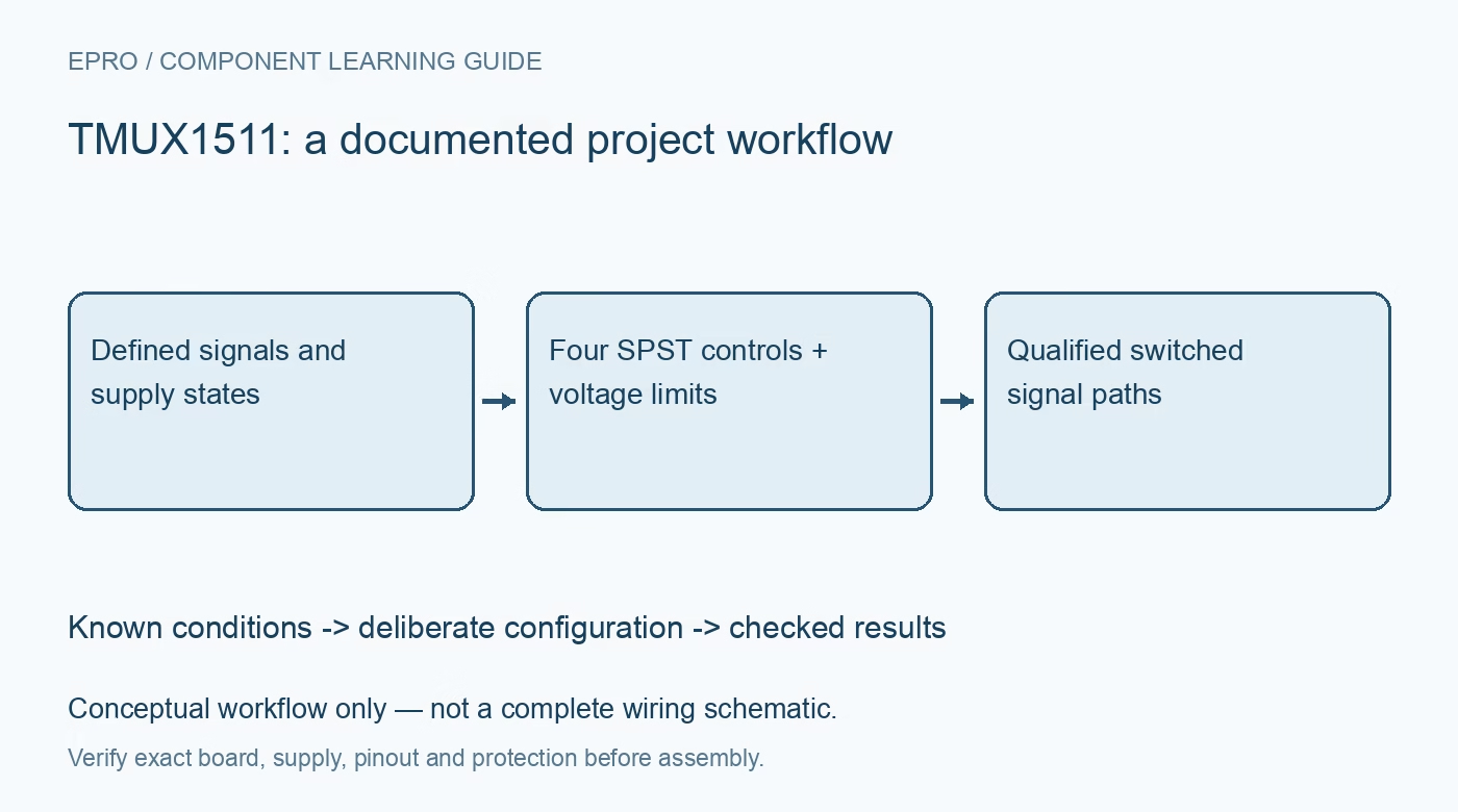
Distinguish TMUX1511 powered signal limits from its 3.6-volt powered-off limit, and qualify four independent SPST paths and control states. This is a documentation-based planning guide, not a report of independent hands-on testing.
1. Map four independent switches rather than a multiplexer
The TMUX1511 contains four independently controlled one-to-one SPST paths. There is no binary address that selects one of four inputs onto a common output. Draw the source, drain and select connection for each channel before routing the board. The paths are bidirectional within their operating limits, but that does not make them galvanic isolators. Define the common reference, signal source impedance and destination loading explicitly, especially when several switched paths belong to different powered subsystems. Manufacturer documentation.
2. Calculate the powered signal envelope from VDD
The recommended supply range is 1.5 to 5.5 volts. With VDD at or above 1.5 volts, the allowed signal range extends from ground to twice VDD, capped at 5.5 volts. For example, a 1.8-volt supply does not permit a five-volt signal merely because five volts is below the overall cap; twice 1.8 volts is 3.6 volts. Evaluate both terminals and the entire waveform, including overshoot, rather than checking only its average value. Manufacturer documentation.
3. Apply the separate unpowered limit during brownout
When VDD is below 1.5 volts, including a fully unpowered condition, the documented source and drain range is zero to 3.6 volts. The five-and-a-half-volt powered signal ceiling must not be carried into that state. A valid normal-operation signal can therefore become invalid during supply collapse. Create a state table for startup, brownout and disconnect events. If the source can remain active, ensure its voltage is bounded appropriately throughout those states or provide a separately reviewed protection arrangement. Manufacturer documentation.
4. Distinguish fail-safe control from signal protection
Select pins have fail-safe logic behavior, but their ratings are separate from the analog-terminal limits. Select high closes the associated switch; low opens it, and internal six-megohm pulldowns establish a default tendency. A weak internal pulldown does not automatically dominate external leakage, coupling or an attached controller. Verify guaranteed logic thresholds and define each control during reset. Do not infer that because a select pin can be driven before VDD, any voltage is also acceptable on an unpowered signal terminal. Manufacturer documentation.
Newest in the store


5. Budget resistance, loading and switching artifacts
A typical on-resistance headline describes particular test conditions, not an ideal zero-ohm connection. Include its variation with supply, signal level and temperature in the signal-error budget. Off-state capacitance, leakage and charge injection also matter when switching high-impedance nodes. Give a newly selected measurement path enough settling time and check the receiving ADC or amplifier requirements. An apparently correct static voltage after several seconds does not establish accurate acquisition immediately after a control transition. Manufacturer documentation.
6. Interpret bandwidth in the intended measurement setup
The gigahertz bandwidth headline is a characterized analog response, not a guaranteed digital data rate through arbitrary wiring and connectors. Source impedance, destination impedance, board geometry and parasitic capacitance change the observed response. Define an amplitude-error or timing criterion and test against that requirement. Keep discontinuities and return paths under control. For a slow sensor path, leakage and settling may be more important than bandwidth; for a fast signal, a breadboard test is not a credible qualification fixture. Manufacturer documentation.
7. Verify every supply and control state systematically
Prepare a matrix covering each path on, off, VDD valid, VDD below its operating range and source still active. Use bounded low-voltage signals and appropriate current limiting, while observing both the signal and any unintended supply rise. Check the rest of the board for alternate back-power paths through protection diodes or peripherals. Save actual measured leakage and settling separately from specified limits. The result should identify valid operating states, not claim universal isolation from a successful single-channel demonstration. Manufacturer documentation.
Related reading: TMUX1101 Analog Switch: 7 Checks for a High-Impedance Signal.
Catalog note: The exact-part search did not return a matching Epro listing during preparation. Check the current catalog; this guide makes no price, availability or included-accessory claim.