


TPS22960 Dual Load Switch: 7 Checks for Shared Slew and Output Discharge

TPS22960 Dual Load Switch: 7 Checks for Shared Slew and Output Discharge
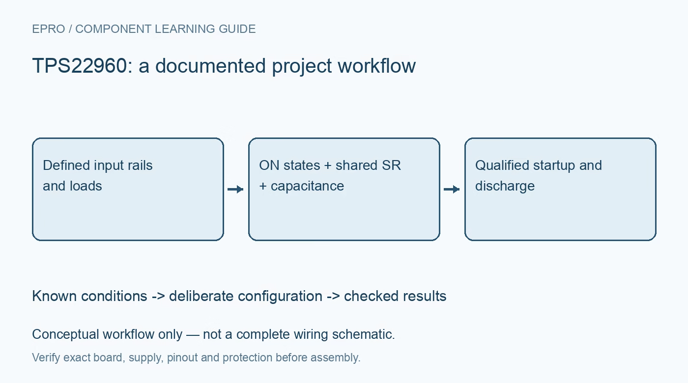
Check TPS22960 dual-channel control, shared slew selection, inrush demand, discharge loading and reverse-current paths before sequencing rails. This is a documentation-based planning guide, not a report of independent hands-on testing.
1. Map the two independent paths and exact package
The TPS22960 contains two controlled P-channel load-switch paths with a recommended input range of 1.62 to 5.5 volts. ON1 and ON2 control their respective channels and must not float. Confirm the package drawing: the SOT and UQFN versions do not share the same pin-number mapping for all signals. Label each input, output, load and bypass capacitor. Two channels in one package do not imply galvanic separation, automatic sequencing or independent protection against every possible cross-powered load state. Manufacturer documentation.
2. Check guaranteed control levels rather than a GPIO slogan
The datasheet application discussion mentions compatibility with common logic systems, but the recommended VIH requirement is 1.4 or 1.5 volts depending on input voltage. A nominal 1.2-volt GPIO therefore does not automatically provide a guaranteed high. Compare minimum controller VOH and maximum VOL against the actual switch requirements under load and temperature. Apply the same care to the shared SR selection. Explicit pull networks and startup states are more defensible than relying on an ambiguous general compatibility statement. Manufacturer documentation.
3. Recognize that slew selection is shared
The SR pin selects the slew behavior of both channels, even though their ON commands are independent. TI gives typical 3.3-volt rise times of 75 microseconds with SR grounded and 660 microseconds with SR high. Those values belong to stated test conditions, not universal startup times for every rail, capacitor or load. If two outputs require different ramp profiles, a single shared selection may not satisfy both. Record the selected state and validate each populated output separately. Manufacturer documentation.
4. Budget inrush instead of calling slew a current limit
Output-capacitor charging demand is approximately capacitance times voltage slew rate, with the operating load added. A slower ramp can reduce that demand, but the device is not a programmable current limiter. The 500-milliamp maximum continuous switch-current rating is a boundary to respect, not an automatic clamp or a universal thermal guarantee. Include simultaneous startup when sizing the source and bypassing. Observe input droop as well as output rise, because an apparently smooth output can conceal stress on an upstream rail. Manufacturer documentation.
Newest in the store


5. Treat quick discharge as a real load on the output
When a channel is disabled, its quick-output-discharge path connects the output to ground through an internal resistor, nominally 85 ohms. Discharge time depends on actual capacitance and any continuing external source. If another peripheral drives the disabled rail, that path can sink current rather than simply empty a capacitor. Identify cross-powered interfaces before assuming a rail reaches zero. Calculate the expected decay only for the conditions where a simple resistor-capacitor model is valid, and check it on the assembled circuit. Manufacturer documentation.
6. Review reverse flow through the intrinsic body diode
The PMOS body diode can conduct if an output rises above its input. Quick discharge and an off command do not establish reverse-current blocking. TI highlights input-removal cases where a larger output capacitor can keep VOUT above VIN. Review the allowed output-to-input relationship, source removal and independently powered loads. Where reverse isolation is required, select a separately suitable arrangement rather than describing a larger input capacitor as a complete blocking solution. Account for all possible stored-energy and external-source paths. Manufacturer documentation.
7. Qualify combined dissipation and sequencing behavior
Estimate conduction loss for both channels using appropriate on-resistance conditions, then check the actual package and board thermal situation. Test one output and both outputs starting, disabling and losing their source with a current-limited low-voltage setup. Record ON levels, SR state, input and output capacitances, load demand and temperature. Separate calculated expectations from measured waveforms. Acceptance should demonstrate valid rail behavior throughout transitions, not merely confirm that both outputs eventually reach their nominal voltages after the transient has passed. Manufacturer documentation.
Related reading: TPS22953 Load Switch: 7 Checks for Bias, Supervision and Reverse Blocking.
Catalog note: The exact-part search did not return a matching Epro listing during preparation. Check the current catalog; this guide makes no price, availability or included-accessory claim.