


OPA817 High-Speed Op Amp: 7 Checks Beyond the 800MHz Headline

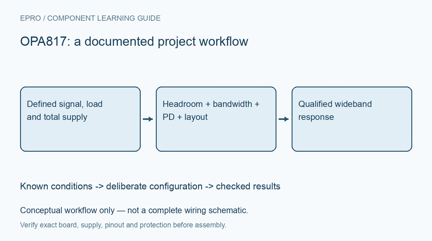
OPA817 High-Speed Op Amp: 7 Checks Beyond the 800MHz Headline
Plan OPA817 buffers with supply and common-mode headroom, realistic large-signal bandwidth, noise integration, PD thresholds and RF-aware layout. This is a documentation-based planning guide, not a report of independent hands-on testing.
1. Match the supply and signal requirements first
The OPA817 operates from six to 12.6 volts total supply, not from an ordinary 3.3-volt logic rail. It supports suitable single or split supplies, but lower-supply operation demands careful input common-mode biasing. Check input and output headroom under the actual load rather than assuming a JFET input or precision headline implies rail-to-rail operation. Define signal amplitude, offset, frequency and destination impedance before selecting gain. Start with bounded low-voltage bench signals and current-limited supplies on an appropriate high-speed board. Manufacturer documentation.
2. Distinguish unity-gain bandwidth from gain-bandwidth product
The device headline includes approximately 800-megahertz unity-gain bandwidth and a 400-megahertz gain-bandwidth product. These describe different characterized aspects of the response and are not interchangeable promises for every gain and layout. Select a passband with an allowed amplitude or phase error, then check the relevant curves and conditions. Unity-gain stable does not mean an arbitrary capacitive load or feedback layout remains flat and well damped. Include the downstream converter, probe and cable network in the actual signal-chain model. Manufacturer documentation.
3. Check large-signal response independently
The small-signal bandwidth does not establish the same performance at a large output swing. Slew rate and distortion impose additional restrictions; the manufacturer separately specifies large-signal bandwidth under stated amplitude and load conditions. For a sine wave, required peak slew is two pi times frequency times peak voltage. Use that relation as an initial feasibility check, not a complete settling or distortion guarantee. Verify output swing and current as well, especially when driving a low impedance or a terminated cable. Manufacturer documentation.
4. Integrate noise over the required bandwidth
A low voltage-noise density becomes a larger total RMS noise when integrated across a wide band. The datasheet provides an illustrative calculation using 4.5 nanovolts per root hertz and a 200-megahertz single-pole bandwidth, giving roughly eighty microvolts RMS with its stated assumptions. Do not interpret the spectral-density number as the total output noise. Add source resistance, feedback-network noise, noise gain and the actual filter response. A high-impedance input configuration may have a different dominant noise contribution than a fifty-ohm measurement setup. Manufacturer documentation.
Newest in the store


5. Reference power-down logic to the positive rail
PD thresholds are specified relative to the positive supply. The table gives guaranteed enabled behavior above the positive rail minus one volt and disabled behavior below the positive rail minus three volts, under its stated conditions. A 3.3-volt controller signal is therefore not automatically a valid enabled state when the positive rail is five volts. Check pin ratings and interface translation before connecting it. Power-down current and wake timing also have conditions; do not accept precision data immediately after changing PD without a suitable recovery assessment. Manufacturer documentation.
6. Treat layout and loading as part of the amplifier
At these speeds, pad capacitance, feedback geometry, return paths and component parasitics materially change response. Follow the manufacturer layout guidance, keep critical connections compact and provide appropriate local decoupling. Evaluate capacitive-load isolation using the relevant guidance rather than attaching a long probe lead or cable directly and blaming the amplifier for ringing. The exposed pad and board copper also matter thermally: typical 23.5-milliamp operating current at ten volts total supply implies about 0.235 watt before output-load effects. Manufacturer documentation.
7. Qualify response with a defined measurement fixture
Record supply rails, bias, gain network, load, termination, bandwidth and instrument connections. Verify DC operating points first, then use suitable low-amplitude steps and sine waves to inspect peaking, settling and distortion within the fixture capability. Check the intended signal amplitude separately from the small-signal sweep. Mark observed results, calculations and datasheet examples distinctly. A solderless breadboard or poorly matched cable setup cannot establish the advertised wideband performance, and a clean low-frequency output does not validate the full high-speed acquisition chain. Manufacturer documentation.
Related reading: OPA320 CMOS Op Amp: 7 Checks for ADC Drive and Suffix Pins.
Catalog note: The exact-part search did not return a matching Epro listing during preparation. Check the current catalog; this guide makes no price, availability or included-accessory claim.