


OPA818 FET-Input Amplifier: 7 Checks for Noise Gain and Input Headroom

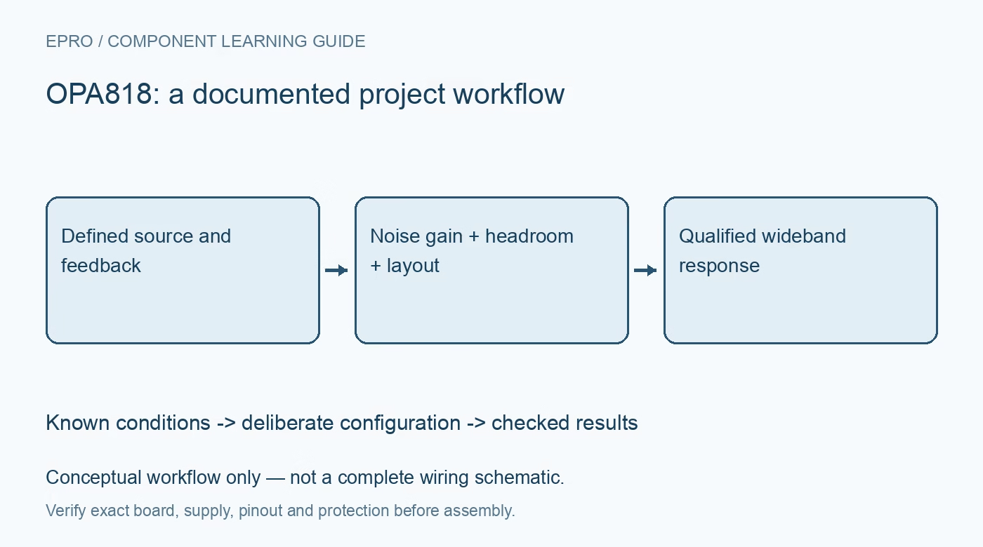
OPA818 FET-Input Amplifier: 7 Checks for Noise Gain and Input Headroom
Review OPA818 decompensation, noise gain, common-mode headroom, TIA capacitance, supply range and high-frequency layout. This is a documentation-based planning guide, not a report of independent hands-on testing.
1. Start with a decompensated amplifier model
OPA818 is a high-speed FET-input voltage-feedback amplifier, not a generic unity-gain buffer. Conventional voltage-gain circuits require a noise gain of at least seven for the documented stability condition. Identify signal gain and noise gain separately, particularly in inverting and transimpedance arrangements. Do not place the device in a follower merely because a simulation initially produces an output. The feedback network and parasitic capacitances determine whether the actual circuit is stable. Manufacturer documentation.
2. Check supply span and common-mode limits together
The supported total supply range is 6 V to 13 V, but a valid supply span does not make every midpoint a valid input common mode. The datasheet specifically cautions that ground is outside the input common-mode range with symmetric plus-and-minus-three-volt supplies. An asymmetric supply arrangement may be needed. Use guaranteed limits at the chosen conditions, not just the typical upper-input headroom, before connecting a ground-referenced sensor or laboratory source. Manufacturer documentation.
3. Budget output swing for the intended load
Output swing depends on supply rails, load and operating conditions. The headline eight-volt peak-to-peak capability is associated with stated conditions and is not available on every supply configuration. Establish the receiver input limits, termination and DC offset before choosing gain. Include transient overshoot and recovery from overload in that review. A circuit can meet its small-signal gain target yet clip on a realistic pulse or drive a downstream converter outside its safe range. Manufacturer documentation.
4. Shape TIA noise gain using total capacitance
For a photodiode transimpedance amplifier, include detector capacitance, amplifier input capacitance, package and PCB parasitics in the feedback design. The low-frequency transimpedance behavior does not directly describe high-frequency noise gain. Choose the feedback capacitor using the manufacturer stability method and evaluate the resulting bandwidth and peaking. A demonstration with a particular photodiode capacitance and feedback resistance is not a universal TIA result. Changing the detector or connector can require a new compensation review. Manufacturer documentation.
Newest in the store


5. Distinguish bandwidth, slew rate and settling
Small-signal bandwidth, gain-bandwidth product, large-signal bandwidth and slew rate describe different limits. The headline 2.7 GHz gain-bandwidth product does not mean arbitrary closed-loop signals remain flat to that frequency. Compare amplitude, gain, load and distortion conditions with the electrical tables. For pulse work, define a settling tolerance and observation window. A fast edge or broad response alone does not demonstrate low distortion, adequate phase margin or accurate recovery after saturation. Manufacturer documentation.
6. Treat the PCB as part of the circuit
At these speeds, feedback trace length, ground geometry, decoupling and output loading materially affect performance. Follow the manufacturer layout guidance and use the correct package footprint and thermal arrangement. Avoid solderless breadboards for a meaningful wideband qualification. Probe capacitance can alter a sensitive summing junction, so choose measurement points and instruments deliberately. Compare a board-level model including practical parasitics with measured behavior rather than treating schematic component values as the complete system. Manufacturer documentation.
7. Qualify operating states before trusting the waveform
Test bounded DC operating points before increasing signal bandwidth or amplitude. Check startup, any available shutdown control for the selected package, overload recovery and the intended output termination. Record rail voltages, gain network, detector capacitance and measurement loading. Look for oscillation outside the apparent signal band as well as visible peaking. Retain both the test conditions and uncertainty; this guide establishes a documentation-based review path, not a claim of independent wideband bench validation. Manufacturer documentation.
Related reading: OPA817 High-Speed Op Amp: 7 Checks Beyond the 800MHz Headline.
Catalog note: The exact-part search did not return a matching Epro listing during preparation. Check the current catalog; this guide makes no price, availability or included-accessory claim.