


TPS63060 Buck-Boost Converter: 7 Checks for Real Load Capability

TPS63060 Buck-Boost Converter: 7 Checks for Real Load Capability
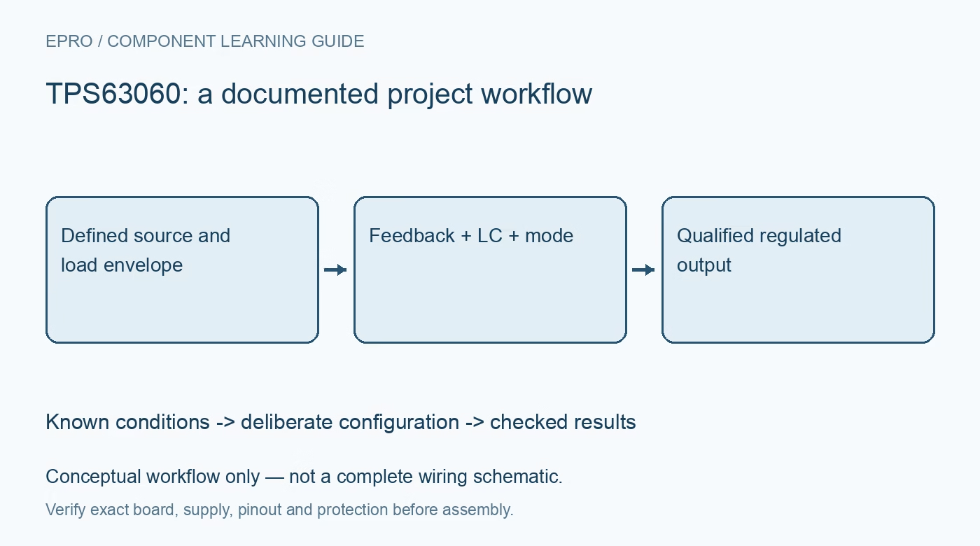
Plan TPS63060 conversion with switch-current limits, input range, feedback, LC selection, operating mode and thermal validation. This is a documentation-based planning guide, not a report of independent hands-on testing.
1. Define the complete input-to-output envelope
TPS63060 is the adjustable member of a synchronous buck-boost family operating from 2.5 V to 12 V input with output settings in the documented 2.5 V to 8 V range. It can transition between step-down and step-up operation, but a valid voltage combination alone does not establish load capability. List minimum input voltage, maximum input voltage, desired output and transient load. Check the exact device identity before using a fixed-output relative’s feedback connections. Manufacturer documentation.
2. Do not convert switch current into an output guarantee
The two-amp switch-current headline is not a promise of two amperes at every boosted output. In boost operation, input and inductor current exceed output current according to the power conversion ratio and losses. The datasheet gives operating-condition-dependent output-current examples. Calculate the worst-case demand at the lowest source voltage, including efficiency and current-limit tolerance. Battery sag and wiring resistance can move the converter into a more demanding condition than the nominal source label suggests. Manufacturer documentation.
3. Set feedback using the adjustable-device equation
Choose the output divider from the manufacturer reference relationship and verify the selected resistor values before enabling the converter. Keep the feedback connection away from switch-node coupling and noisy power returns. Include divider tolerance and regulator accuracy in the predicted rail range. A divider copied from a fixed-output family drawing can be wrong for this part. Treat the calculated output as a target to be measured under load, not as an independently verified result. Manufacturer documentation.
4. Select the inductor and capacitors as a qualified network
Use the documented combinations of inductance and effective output capacitance rather than choosing each component in isolation. Check inductor saturation current, RMS heating, DC resistance and actual bias-dependent capacitance. The reference application uses specific parts and conditions that do not automatically transfer to another PCB. Place local bypassing and power components according to the layout guidance. Nominal microfarads printed on a capacitor do not establish its effective value at the intended operating voltage. Manufacturer documentation.
Newest in the store


5. Choose power-save or forced switching intentionally
The device supports power-save operation for light-load efficiency and forced fixed-frequency operation through the documented PS/SYNC control behavior. Review the pin requirements before driving it from a controller or external synchronization source. The operating mode changes ripple, frequency behavior and light-load consumption. Compare those consequences with the downstream sensor or radio requirements. An efficiency figure or switching-frequency headline should always retain its mode and load conditions rather than becoming a universal board specification. Manufacturer documentation.
6. Interpret enable, load disconnect and power good separately
EN controls operation, and shutdown disconnects the load from the input as described by the device architecture. That feature is not galvanic isolation or a blanket guarantee for every externally driven output condition. Review the documented power-good thresholds and open-drain interface before using PG for sequencing. A digital status transition does not establish output noise or transient accuracy. Define safe behavior if the source collapses, the load remains powered elsewhere or the controller resets. Manufacturer documentation.
7. Validate the worst power points on the real PCB
Begin with a current-limited source and moderate resistive or electronic load. Sweep input voltage across buck, transition and boost regions while monitoring output regulation, input current and component temperature. Exercise realistic load steps and startup capacitance. Use suitable probing to avoid mistaking probe-loop pickup for converter ripple. Record inductor, capacitors, mode, ambient conditions and load profile. These observations qualify one implementation; they cannot be inferred from the ideal power balance or a reference efficiency curve alone. Manufacturer documentation.
Related reading: TPS63070 Buck-Boost: 7 Checks Across the Input-Output Boundary.
Catalog note: The exact-part search did not return a matching Epro listing during preparation. Check the current catalog; this guide makes no price, availability or included-accessory claim.