


OPA858 FET Amplifier: 7 Checks for Noise Gain and Detector Capacitance

OPA858 FET Amplifier: 7 Checks for Noise Gain and Detector Capacitance
Plan OPA858 transimpedance circuits with valid noise gain, low-bias assumptions, headroom, feedback capacitance and power-down limits. This is a documentation-based planning guide, not a report of independent hands-on testing.
1. Treat the device as decompensated, not a follower
OPA858 is a FET-input amplifier with a 5.5 GHz gain-bandwidth headline and conventional stability at noise gains of seven or more. That does not make it a unity-gain-stable buffer. Establish signal gain and noise gain separately, especially for a photodiode transimpedance stage. A low-frequency transfer equation alone says little about high-frequency phase margin. The detector, feedback network and parasitic capacitances must be included before assuming the circuit can produce a clean pulse response. Manufacturer documentation.
2. Verify supply and the actual DC operating point
The recommended supply span is 3.3 V to 5.25 V. Input common-mode and output swing still have their own limits and conditions; the input range including the negative supply does not make the output rail-to-rail. Set a valid detector or signal midpoint and compare the full waveform with guaranteed limits. Check the receiving instrument or ADC as well. A valid supply and small input can coexist with an output offset that leaves inadequate room for the intended pulse amplitude. Manufacturer documentation.
3. Put the low-bias figure in its measurement context
The ten-picoampere input-bias headline is attractive for sensitive detectors, but it is not the only source of DC or noise error. Use the specified temperature behavior and include detector dark current, board leakage, contamination and feedback-resistor effects. Distinguish input current noise from average bias current and voltage noise. A clean PCB and suitable guarding may matter as much as the nominal amplifier number. Do not infer an assembled system’s minimum detectable signal from one typical front-page value. Manufacturer documentation.
4. Choose feedback capacitance from the complete TIA model
Include detector capacitance, amplifier common-mode and differential input capacitance, package parasitics and board geometry when designing compensation. Noise gain changes with frequency, so selecting only a transimpedance resistor is insufficient. Follow the manufacturer stability procedure and compare peaking, bandwidth and settling under realistic conditions. A reference circuit with a particular detector capacitance is an example, not a reusable performance guarantee. Changing a connector or probe can materially affect a high-speed summing node. Manufacturer documentation.
Newest in the store


5. Keep bandwidth, amplitude and settling requirements distinct
The gain-bandwidth product is not a closed-loop bandwidth available at every gain or output amplitude. Check small-signal response, large-signal behavior, slew rate and distortion under conditions comparable to the intended application. For optical pulses, specify acceptable overshoot and baseline settling as well as rise time. A visually fast edge can still hide ringing or overload recovery. Do not translate a reference TIA bandwidth into a general claim for every detector and feedback value. Manufacturer documentation.
6. Define power-down levels relative to the negative rail
The PD disable and enable thresholds are referenced to the negative supply, so a controller’s ground-referenced logic needs a separate compatibility review in a split-supply system. Follow the documented power-down input and output behavior and any source-protection requirements. Shutdown reduces amplifier consumption but is not galvanic disconnection of the detector network. Allow the enable response and analog settling before accepting data. A control pin changing state does not prove immediate measurement readiness or harmless operation under every driven-input condition. Manufacturer documentation.
7. Qualify the PCB, instrument loading and detector together
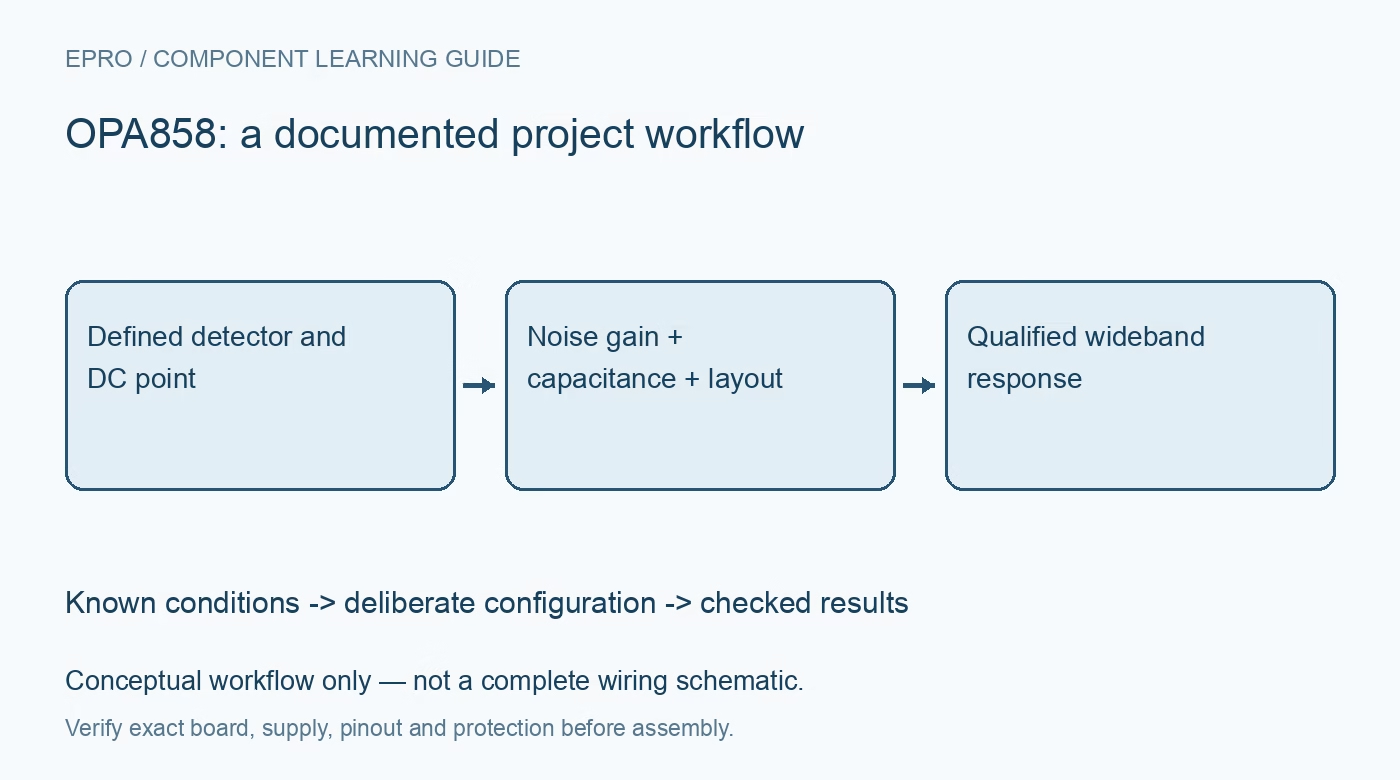
Use the recommended high-frequency layout, short feedback paths and local bypassing. A solderless breadboard cannot establish the intended wideband performance. Begin with bounded DC conditions, then increase pulse amplitude and repetition rate while observing oscillation, peaking and recovery. Include instrument termination and probe capacitance in the model and saved test conditions. Record detector, supply rails, feedback parts and temperature. This workflow proposes implementation-specific evidence and does not claim independent bench validation from the manufacturer example curves. Manufacturer documentation.
Related reading: OPA855 Bipolar Amplifier: 7 Checks for Noise Gain and Bias Current.
Catalog note: The exact-part search did not return a matching Epro listing during preparation. Check the current catalog; this guide makes no price, availability or included-accessory claim.