


UCC27325 Gate Driver: 7 Checks for Mixed Output Polarity

UCC27325 Gate Driver: 7 Checks for Mixed Output Polarity
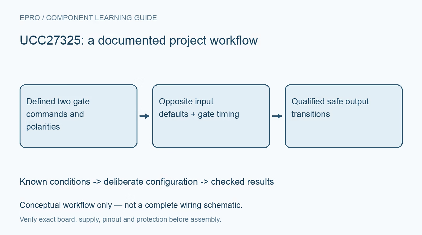
Plan UCC27325 gate drive with its inverting A channel, noninverting B channel, opposite safe input states and independent timing protection. This is a documentation-based planning guide, not a report of independent hands-on testing.
1. Write the two different channel truth tables
UCC27325 has one inverting channel and one noninverting channel. Channel A inverts its input, while channel B preserves the input logic sense. It is not a drop-in logical equivalent of a dual-noninverting family member. Build a separate input-to-output table for each channel and compare it with the intended transistor arrangement. A shared firmware command name such as disabled is not enough to prove both gates become low, because the electrical input levels needed to produce that result are different. Manufacturer documentation.
2. Choose opposite input defaults for low outputs
For this device, holding the inverting A output low requires a high input, whereas holding the noninverting B output low requires a low input. Follow the manufacturer requirement to tie unused inputs to a defined rail rather than leaving them floating. Include controller reset, disconnected control wiring and logic-supply loss in the state table. Applying identical pulldowns to both inputs can create opposite gate states. Establish the safe output condition from the actual truth table rather than from a general assumption that low inputs always mean off. Manufacturer documentation.
3. Confirm the exact pins and absence of enable controls
In the eight-pin mapping, INA is pin two, INB pin four, OUTA pin seven, OUTB pin five and VDD pin six. Pins one and eight have no internal connection, not independent enable functions. Verify the exact package and any exposed-pad connection before assembly. Do not import a newer driver symbol with separate shutdown pins and expect software to control nonexistent terminals. If the power stage requires an emergency disable function, implement and qualify a suitable system-level path instead of assuming the package provides one. Manufacturer documentation.
4. Separate logic thresholds from the gate supply
The input thresholds are compatible with logic-level control and do not track the driver supply in the same way as supply-dependent CMOS threshold drivers. Check their guaranteed limits against the controller outputs. Independently, the recommended gate-driver supply range is 4.5 V to 15 V, and output amplitude follows that rail. Match it to the transistor gate-source rating and intended enhancement. A valid low-voltage control signal does not reduce the voltage applied at the gate or establish adequate immunity to a disturbed gate-return reference. Manufacturer documentation.
Newest in the store


5. Preserve fast logic edges and budget gate charge
The input stage expects digital transitions with suitably short rise and fall times. Do not use a slowly changing RC input waveform as an improvised gate-slew controller; threshold-region behavior can cause unwanted output switching. Evaluate gate resistance in the output path when controlled transistor edges are required. The four-ampere drive headline is a peak capability, not a continuous load rating. Calculate charge delivery, frequency-dependent demand and package dissipation for both channels before selecting bypassing and the upstream driver supply. Manufacturer documentation.
6. Do not confuse complementary polarity with interlock
An inverting and a noninverting output can be useful in a control arrangement, but the device does not thereby provide guaranteed nonoverlap or shoot-through prevention. Check command relationships, propagation limits and transistor turn-off behavior as separate requirements. Ground-referenced low-side drive is also not galvanic isolation or automatic high-side level shifting. Keep gate loops compact and return them to the appropriate transistor source. Any claim that the pair switches safely must include the surrounding power topology and controller behavior, not merely the opposing logic labels. Manufacturer documentation.
7. Validate reset transitions before applying load energy
With a current-limited supply and safe representative gate loads, verify each channel polarity and its reset default. Then check both channels together during controller startup, shutdown and any intended command transition. Observe gate-source waveforms at the transistors and confirm that the independently designed protection works. This article reports no measured switching or fault-response results. Preserve input defaults, driver voltage and timing observations so the accepted behavior can be reproduced rather than inferred from the familiar family package. Manufacturer documentation.
Related reading: UCC27324 Gate Driver: 7 Checks Before Driving Two MOSFETs.
Catalog note: The exact-part search did not return a matching Epro listing during preparation. Check the current catalog; this guide makes no price, availability or included-accessory claim.