


UCC27324 Gate Driver: 7 Checks Before Driving Two MOSFETs

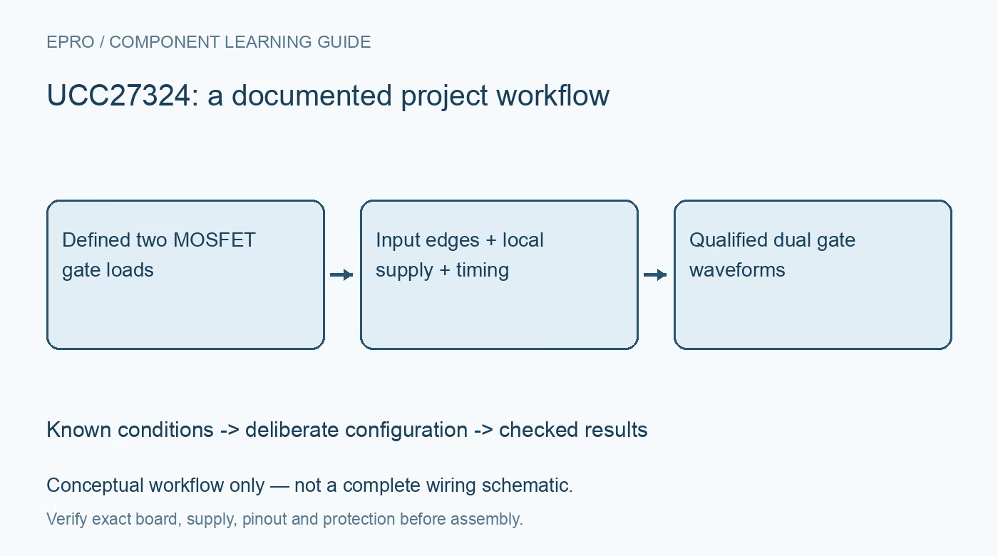
UCC27324 Gate Driver: 7 Checks Before Driving Two MOSFETs
Check UCC27324 dual noninverting gate drive through exact pins, fixed logic thresholds, input edge quality and gate-loop power. This is a documentation-based planning guide, not a report of independent hands-on testing.
1. Select the noninverting member of the driver family
UCC27324 is the dual-noninverting member of a family that also includes different inversion arrangements. Confirm the full part number before deriving output states from an adjacent datasheet example. In the eight-pin mapping, INA is pin two, INB pin four, OUTA pin seven, OUTB pin five and VDD pin six. Pins one and eight have no internal connection; they are not enable inputs. Do not transfer an enable-equipped relative symbol onto this device without checking every terminal. Manufacturer documentation.
2. Review fixed thresholds without confusing gate amplitude
The input thresholds are logic compatible and independent of the driver supply, unlike drivers whose CMOS thresholds track VDD. Compare the guaranteed high and low limits with the controller output under load and temperature. Separately, the gate output amplitude follows the driver supply, whose recommended range is 4.5 V to 15 V. A suitable controller input level does not limit the MOSFET gate-source voltage. Check the transistor enhancement requirement and gate rating before choosing the driver rail. Manufacturer documentation.
3. Drive unused inputs to defined states
The manufacturer explicitly requires unused inputs to be tied to VDD or ground rather than left floating. For a noninverting channel intended to remain off, choose the corresponding low command and ensure that the controller reset state preserves it. These are ordinary driver inputs, not a separate shutdown interface. Define how the overall power stage remains safe during logic power loss and rail sequencing. Do not claim an undocumented lockout or interlock function to fill a gap in the system protection design. Manufacturer documentation.
4. Keep input edges fast and shape the gate externally
The input stage is designed for digital signals with short rise and fall times. The documentation warns that slow-changing inputs can produce repeated high-frequency switching around the threshold. Do not create a delayed or slowed gate waveform by adding an arbitrary large RC network to the logic input. If the MOSFET requires slower gate edges, evaluate appropriate resistance in the driver-to-gate path. Keep timing qualification distinct from intentional gate-slew control and include any external logic or translator behavior in the input-edge review. Manufacturer documentation.
Newest in the store


5. Convert peak drive capability into a power budget
The four-ampere source and sink capability describes peak gate-charge delivery, especially through switching transitions. It is not a continuous output supply rating. Calculate average gate-drive demand from transistor charge, drive voltage and switching frequency, then include driver dissipation and external gate-resistor losses. Use the actual package thermal information rather than assuming identical cooling across SOIC and exposed-pad implementations. When two channels switch, their combined demand also loads the local bypass network and upstream driver rail. Manufacturer documentation.
6. Treat layout and dead time as separate design problems
A short output trace is helpful only when its return loop is also controlled. Place bypassing close to VDD and ground and reference the driver return to the appropriate MOSFET source. The two independent channels do not provide guaranteed dead time or prevent conflicting commands. For complementary power switching, account for device delays, gate discharge and controller behavior independently. This low-side driver also provides neither galvanic isolation nor automatic high-side level shifting, so those functions require a suitable architecture elsewhere. Manufacturer documentation.
7. Verify both channels before connecting significant energy
Begin with a current-limited driver supply and a safe representative gate load. Check input and output polarity, amplitude, transition behavior and the response to controller reset. Inspect gate-source voltage at each transistor rather than measuring only at a remote driver ground. Progress to a powered load only after its protection and command timing are established. This article supplies no independently measured waveforms or switching-loss results; retain the actual test conditions and observations before accepting the final two-channel design. Manufacturer documentation.
Related reading: UCC27527 Gate Driver: 7 Checks for Supply-Dependent Logic.
Catalog note: The exact-part search did not return a matching Epro listing during preparation. Check the current catalog; this guide makes no price, availability or included-accessory claim.