


OPA861 OTA: 7 Checks for a Voltage-Controlled Current Stage

OPA861 OTA: 7 Checks for a Voltage-Controlled Current Stage
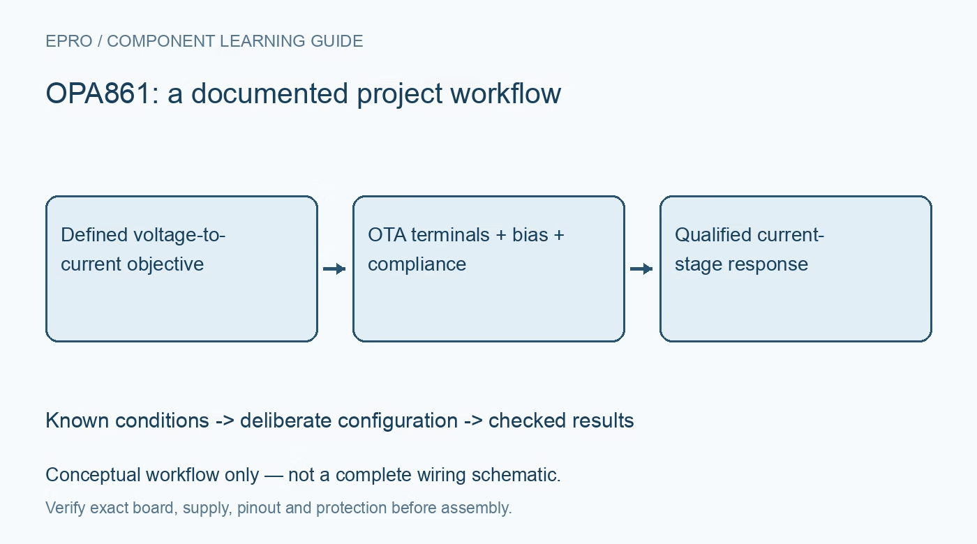
Plan OPA861 circuits with the correct OTA terminals, package mapping, bias resistor, output compliance and load-dependent response. This is a documentation-based planning guide, not a report of independent hands-on testing.
1. Start with an OTA rather than a voltage-op-amp model
OPA861 is an operational transconductance amplifier: its input relationship controls an output current. It does not include the independent voltage buffer found in a related product. Identify the base-like, emitter-like and collector-like terminals and define the external circuit function before borrowing a familiar op-amp symbol. Transconductance has units of amperes per volt, not voltage gain. A circuit may convert that current to voltage through its load, but the load and terminal operating conditions are part of the function, not an afterthought. Manufacturer documentation.
2. Use the exact package pin arrangement
The SO-8 and SOT23-6 packages use different terminal numbering. In the larger package, connections that might resemble a buffer input or output on another device are not an included second amplifier here. Check the manufacturer pin configuration and any no-connect terminals before making a footprint or adapter. Label functional terminals explicitly in the schematic rather than preserving misleading voltage-amplifier names. A correct mathematical circuit can still fail immediately if a compact package is rotated or a related-device pinout is transferred without review. Manufacturer documentation.
3. Define input behavior and output compliance together
The OTA collector supplies a controlled current only within the permitted voltage and current conditions. Determine where that current flows, the resulting collector voltage and the emitter-node behavior over the full signal range. Check supply headroom and the actual load rather than multiplying a headline transconductance by an arbitrary input amplitude. The signal is bipolar around its operating point under suitable conditions, but that does not establish unrestricted terminal swings. Include startup and a disconnected load in the compliance review. Manufacturer documentation.
4. Install the required bias-adjustment network
The adjustment resistor connects from the IQ-adjust terminal to the negative supply and sets OTA bias behavior. The documentation gives a recommended adjustment range and example tradeoffs; application sketches can omit details that the complete circuit still needs. Choose a defined resistor and preserve its value with the calculations. Changing bias changes transconductance, bandwidth and current consumption, so it is not merely a power-saving adjustment that leaves the transfer function unchanged. Do not interpret the terminal as an ordinary digital enable. Manufacturer documentation.
Newest in the store


5. Keep supply examples separate from guaranteed application behavior
Manufacturer characterization includes specific supply, load and adjustment-resistor conditions, including split-supply examples. Compare the required input range, collector swing and load current with the applicable electrical limits at the selected rails. A supported supply voltage does not alone prove linear behavior for the proposed source and load. If the circuit uses a single supply and a bias point, analyze every relevant terminal relative to that point. Do not apply a ground-centered example unchanged to a differently biased implementation. Manufacturer documentation.
6. Budget bandwidth through the whole current stage
The useful response depends on bias, operating configuration, load impedance and parasitic capacitance. A headline open-loop bandwidth at a stated gain is not a guaranteed closed-loop bandwidth for every current-source or filter application. Follow the high-frequency layout and bypassing guidance and include collector-node capacitance in the model. Long wiring or a solderless breadboard can dominate the result. Evaluate source and measurement loading as part of the circuit so an apparent bandwidth limit is not attributed to the OTA without evidence. Manufacturer documentation.
7. Qualify DC transfer before pursuing high-frequency claims
With a suitable limited test setup, establish bias currents and node voltages, then verify the intended voltage-to-current relationship over a safe range. Check the actual load response and recovery from an allowed over-range condition before measuring frequency behavior. Record supplies, resistor values and fixture conditions with each observation. This guide reports no independently measured transconductance or bandwidth. Keep the distinction between a calculated function and observed performance clear so later load or bias changes receive a focused review. Manufacturer documentation.
Related reading: OPA860 OTA and Buffer: 7 Checks Before Choosing a Circuit.
Catalog note: The exact-part search did not return a matching Epro listing during preparation. Check the current catalog; this guide makes no price, availability or included-accessory claim.