


OPA860 OTA and Buffer: 7 Checks Before Choosing a Circuit

OPA860 OTA and Buffer: 7 Checks Before Choosing a Circuit
Plan OPA860 circuits by separating transconductance and buffer functions, bias adjustment, compliance limits and high-frequency layout. This is a documentation-based planning guide, not a report of independent hands-on testing.
1. Separate the OTA from the independent voltage buffer
OPA860 combines an operational transconductance amplifier with an uncommitted unity-gain buffer. They are different circuit blocks with different input and output behavior, not one conventional voltage op amp with interchangeable terminals. The OTA uses base-like, emitter-like and collector-like terminals, while the buffer has its own input and output. Draw the required signal flow explicitly before adopting an application circuit. A high buffer bandwidth figure must not be assigned automatically to the OTA or to a complete external feedback network. Manufacturer documentation.
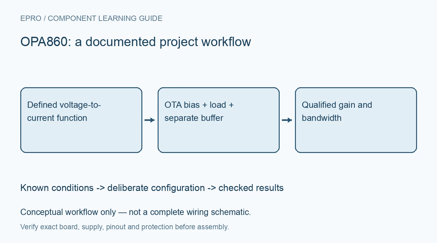
2. Treat transconductance as a voltage-to-current relationship
The OTA converts its input relationship into collector current; transconductance is expressed in amperes per volt, not ordinary voltage gain. The external load and feedback arrangement determine how that current becomes a useful voltage or other circuit function. Define the intended signal polarity, current range and load impedance. Check collector compliance and the emitter-node behavior against the electrical specifications. Simply attaching a resistor and multiplying by a headline transconductance value does not establish linear operation over arbitrary input amplitudes. Manufacturer documentation.
3. Use the actual supply and operating conditions
Much of the manufacturer characterization is given at plus and minus five-volt supplies with specified loading and bias adjustment. Do not treat absolute-maximum supply ratings as a recommended design point or assume a low-voltage single-supply controller environment is automatically compatible. Review input ranges, output swing and current at the selected rails. Establish an appropriate signal reference for both blocks and account for source and load ground relationships. Safe supply operation alone does not guarantee that every internal terminal has adequate voltage headroom. Manufacturer documentation.
4. Configure the quiescent-current adjustment deliberately
The external adjustment resistor connects from the IQ-adjust pin to the negative supply and controls the OTA bias behavior. The buffer bias circuitry is independent, so reducing OTA bias does not shut down all device consumption. The documentation provides an adjustment range and example conditions for bandwidth, transconductance and current tradeoffs. Select a defined resistance and keep it with the circuit calculations. Do not interpret the adjustment terminal as a generic logic enable or change bias without reconsidering the expected AC response and gain. Manufacturer documentation.
Newest in the store


5. Distinguish buffer speed from loaded circuit bandwidth
The buffer has a very high small-signal bandwidth under stated conditions, while the OTA has its own gain- and load-dependent response. Capacitive loads, output amplitude and the chosen bias setting change the useful behavior of the complete circuit. Establish the required closed-loop response and allowable peaking before comparing headline numbers. Where the buffer drives a cable or ADC network, evaluate isolation resistance and load behavior from the applicable guidance rather than assuming a fast unity-gain block is stable with every external capacitance. Manufacturer documentation.
6. Build the high-frequency return paths into the design
Place bypass capacitors close to the supply terminals and follow the recommended layout approach for sensitive nodes and output loading. Include pad and trace capacitance in the OTA collector and feedback analysis. Keep source and load return paths from injecting current into the signal reference. A solderless breadboard or long jumper wiring is not a representative implementation for evaluating the published high-frequency behavior. Review the exact package orientation because the OTA terminals and independent buffer connections can otherwise be confused during assembly. Manufacturer documentation.
7. Qualify current transfer and voltage response separately
Begin with limited supplies and safe low-amplitude signals, checking bias currents and node voltages before pursuing bandwidth. Verify the OTA transfer relationship under the actual load, then characterize the buffer and complete circuit response. Record supply rails, adjustment resistance, amplitude and fixture conditions. This guide reports no independently measured transconductance or frequency response. Preserve the distinction between calculated circuit function and observed performance so later bias or load changes receive a targeted review instead of inheriting an unsupported bandwidth claim. Manufacturer documentation.
Related reading: OPA859 FET Amplifier: 7 Checks Beyond Unity-Gain Stability.
Catalog note: The exact-part search did not return a matching Epro listing during preparation. Check the current catalog; this guide makes no price, availability or included-accessory claim.