


OPA859 FET Amplifier: 7 Checks Beyond Unity-Gain Stability

OPA859 FET Amplifier: 7 Checks Beyond Unity-Gain Stability
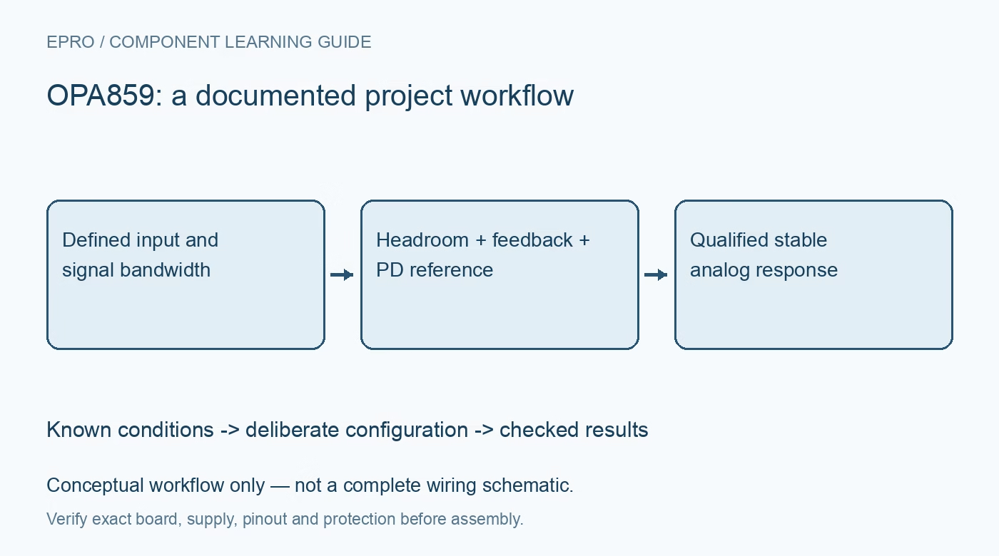
Plan OPA859 amplifier stages with distinct bandwidth definitions, input headroom, detector capacitance and referenced power-down control. This is a documentation-based planning guide, not a report of independent hands-on testing.
1. Separate unity-gain stability from a bandwidth promise
OPA859 is unity-gain stable, unlike a related decompensated amplifier that requires a higher noise gain. Its headline 1.8 GHz unity-gain bandwidth and 900 MHz gain-bandwidth product are different specifications, not interchangeable descriptions. Read their measurement conditions before estimating a circuit response. Unity-gain stability also does not guarantee freedom from ringing with every capacitive load or detector network. Define signal bandwidth, allowable peaking and amplitude first, then select the feedback arrangement for that requirement. Manufacturer documentation.
2. Check input common mode and output swing independently
The amplifier uses a 3.3 V to 5.25 V total supply range. Its input capability includes the negative rail under specified conditions, but the positive side needs headroom. The output also has load-dependent swing limits. A single-supply signal centered at an inconvenient bias can violate one of these limits even when its amplitude seems small. Check both inputs and the requested output against the actual rails, including startup, overload and detector-disconnected conditions rather than relying on a generic rail-to-rail label. Manufacturer documentation.
3. Interpret FET input bias within the complete error budget
Low typical input bias current is useful when the signal source has high impedance, but it is not the only source of offset or noise. Include temperature dependence, board leakage, resistor noise and voltage noise interacting with circuit impedance. Compare specifications under their stated conditions instead of multiplying a typical room-temperature value into a guaranteed application limit. Clean routing and suitable insulation can matter as much as the amplifier headline when a small detector current must remain distinguishable from leakage. Manufacturer documentation.
4. Compensate detector capacitance rather than assuming stability
For transimpedance use, combine detector capacitance, input capacitance, package effects and board parasitics when shaping the feedback network. The compensation capacitor trades bandwidth against stability and noise behavior; it is not chosen solely from the desired DC gain resistor. Use the manufacturer analysis and a suitable model to establish a starting design, then evaluate the physical circuit. A unity-gain-stable voltage amplifier can still require careful transimpedance compensation because the frequency-dependent noise gain is a separate design consideration. Manufacturer documentation.
Newest in the store


5. Treat layout as part of the feedback circuit
Short feedback connections, appropriate bypassing and a controlled return structure are essential at these speeds. Check the package-specific connections, including the WSON thermal-pad requirement to connect to the negative supply. Do not copy an exposed-pad ground convention from an unrelated device when using split rails. Limit stray capacitance at sensitive inputs and include the output load and measurement probe in the circuit model. A solderless breadboard is not a representative implementation of a high-frequency manufacturer evaluation layout. Manufacturer documentation.
6. Reference power-down control to the negative supply
The PD thresholds are defined relative to the amplifier negative rail. Their relationship to controller ground therefore changes when the amplifier moves from a grounded single supply to split supplies. Verify the electrical threshold limits and permitted control voltage rather than assuming a fixed microcontroller logic connection works in every arrangement. Include the transition from power-down to active operation in the settling policy. A high-impedance disabled output should not be mistaken for an actively regulated output at the desired bias. Manufacturer documentation.
7. Check amplitude, recovery and loading with stated conditions
Evaluate a small signal first, then the largest intended amplitude, step response and overload recovery with the real source and output load. Record bandwidth, probe arrangement and supply conditions with each result. Compare simulations and datasheet examples as planning evidence, not as measurements of a new board. This guide contains no independent performance claim. A useful final record distinguishes stable small-signal behavior from acceptable large-signal behavior and identifies which observations remain valid after changing the detector, cable or ADC input network. Manufacturer documentation.
Related reading: OPA858 FET Amplifier: 7 Checks for Noise Gain and Detector Capacitance.
Catalog note: The exact-part search did not return a matching Epro listing during preparation. Check the current catalog; this guide makes no price, availability or included-accessory claim.