


ADS127L11 Precision ADC: 7 Checks for Filter Latency, Buffers and CRC

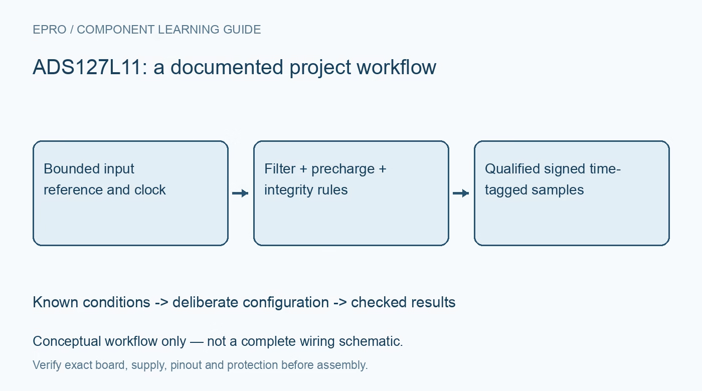
ADS127L11 Precision ADC: 7 Checks for Filter Latency, Buffers and CRC
Plan ADS127L11 acquisition with explicit filter modes, supply-dependent input limits, precharge buffers and separate SPI and register CRC checks. This is a documentation-based planning guide, not a report of independent hands-on testing.
1. Define the supply and signal envelope first
ADS127L11 is a single-channel precision delta-sigma ADC with distinct analog and digital supply requirements. High-speed and low-speed operation have different allowed analog-supply conditions. Check each input pin against the selected rails as well as the differential input range and reference configuration. A differential signal within full scale can still violate an individual pin limit. Begin with protected low-voltage sources and a documented common-mode bias rather than treating an application drawing as a complete wiring or protection design. Manufacturer documentation.
2. Choose the filter for the measurement
The wideband filter prioritizes frequency-domain behavior, while the low-latency options prioritize time-domain response. The headline rates differ: up to 400kSPS for the wideband filter and approximately 1.067MSPS for low-latency operation under the specified conditions. These are not interchangeable settings with identical bandwidth, noise and delay. Record the speed mode, oversampling ratio and filter selection together. Select from the documented response curves and timing tables rather than choosing only the fastest output rate. Manufacturer documentation.
3. Budget filter settling after a change
Output data rate is not the same as the delay before a new input or configuration is fully represented. Include digital-filter latency and settling when scheduling a channel change, starting a conversion sequence or accepting data after reset. Keep timestamps meaningful by recording what event they represent. A stream of plausible samples can still contain transitional filter history. Establish how many observations must be discarded or flagged under the chosen mode instead of copying a fixed discard count from an unrelated ADC. Manufacturer documentation.
4. Check precharge buffers against headroom
Input and reference precharge buffers reduce some dynamic drive demands, but they alter the allowed voltage conditions. For example, enabled analog-input precharge buffers require margin from the analog rails, and the enabled positive-reference buffer has its own upper-headroom requirement. Review those limits before enabling a feature that appears helpful. A buffer option is not an isolation barrier or an overvoltage protector. Qualify the actual source, reference decoupling and sampling configuration together rather than assuming a high-impedance DC reading proves compatibility. Manufacturer documentation.
Newest in the store


5. Separate SPI CRC from register-map CRC
SPI CRC checks transmitted command and output data according to defined byte coverage. The register-map CRC checks configuration contents and must be updated when protected registers change. They solve different problems. The documented SPI polynomial is CRC-8-ATM, but initialization, status inclusion and padding rules still matter. Build known-good and deliberately corrupted test frames for the actual mode. Handle latched error flags as specified; a configuration integrity flag does not by itself restore the intended register values. Manufacturer documentation.
6. Decode data and acquisition state together
Conversion data is transmitted most significant bit first in two’s-complement form, with selectable output resolution and optional status or CRC fields. Remove the non-conversion bytes before sign extension and use the correct reference and range scaling. Confirm known zero, positive and negative inputs with an independent bounded source. Track data-ready state and avoid reporting the same conversion twice. Keep modulator saturation and other relevant status alongside the sample instead of converting every received byte pattern into an apparently valid voltage. Manufacturer documentation.
7. Validate throughput without overstating precision
Check the complete readout path at the intended rate, including firmware latency, clocking, integrity checks and storage. Use appropriate analog antialias filtering; the digital filter does not guarantee immunity to every out-of-band input. Log clock source, supply mode, filter, reference, raw data, timestamps and errors during repeatable tests. The 24-bit output format does not promise 24 noise-free bits in every configuration. Report actual measured conditions and uncertainty separately from manufacturer characterization and this documentation-based planning workflow. Manufacturer documentation.
Related reading: ADS127L01 ADC: 7 Checks for Filter Timing and Valid Data Frames.
Catalog note: The exact-part search did not return a matching Epro listing during preparation. Check the current catalog; this guide makes no price, availability or included-accessory claim.