


ATmega328P Pinout Guide for Arduino Boards

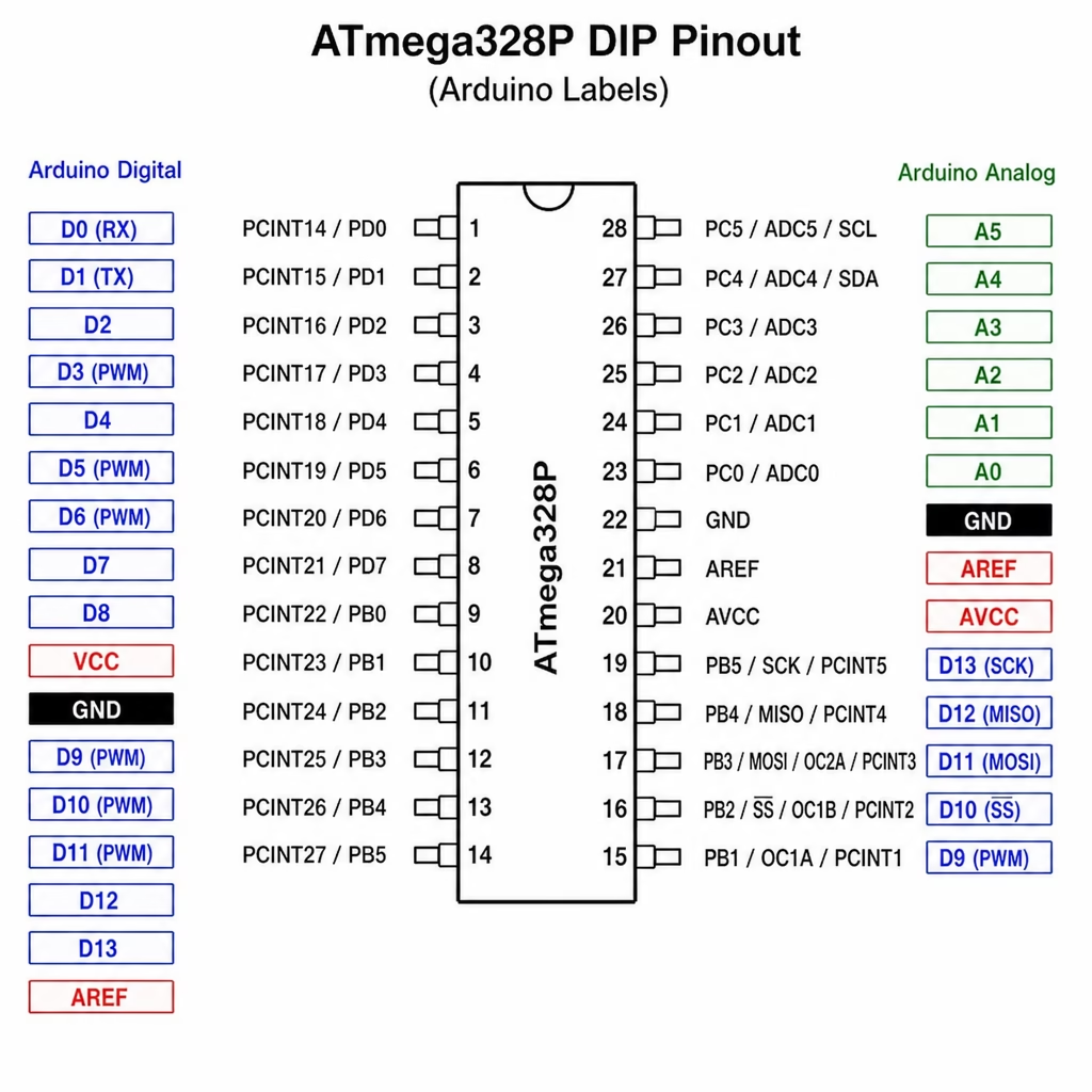
ATmega328P Pinout Guide for Arduino Boards
The ATmega328P is the small 8-bit AVR chip behind the classic Arduino Uno and many Arduino Nano boards. Its raw pin numbers do not match the Arduino header labels. Reading the ATmega328P pinout the right way helps you wire sensors, power rails, clocks, reset parts, and data buses without guesswork. This guide covers the ATmega328P pins, the atmega328p layout, and the main labels you will see on an Arduino pinout ATmega328P diagram.

What the ATmega328P pinout shows
An ATmega328P pinout shows each physical package pin and the jobs it can do: digital I/O, analog input, PWM output, interrupts, clock pins, reset, power, and serial links. One pin can have several names, such as PB3, MOSI, OC2A, and Arduino digital pin 11.
That overlap is normal. The ATmega328P datasheet uses chip-level names, while an Arduino pinout uses board names. The Arduino Uno Rev3, for example, is based on the ATmega328P and exposes 14 digital I/O pins, six analog inputs, six PWM-capable pins, USB, power input, reset, and an ICSP header. (docs.arduino.cc)
When you read an ATmega328P diagram, keep three layers separate:
- Physical pin number: the leg or pad on the package.
- Port name: the AVR register name, such as PB5, PC4, or PD2.
- Arduino label: the board name in sketches, such as D13, A4, or TX.
Mixing those layers is one of the fastest ways to miswire a project, especially when you move the chip off an Uno-style board and onto a breadboard.
Core ATmega328P specs that matter in real projects
The ATmega328P is popular because it is simple, has enough memory for small jobs, and has a large support base. Key ATmega328P specs include 32 KB flash, 2 KB SRAM, 1 KB EEPROM, 23 programmable I/O lines, timers, PWM, serial blocks, ADC channels, a watchdog, and low-power modes. (ww1.microchip.com)
For practical design work, these ATmega328P features matter most:
- Memory: 32 KB flash for code, 2 KB SRAM for runtime data, and 1 KB EEPROM for saved settings.
- I/O: Up to 23 general-purpose chip pins, depending on package and clock setup.
- Analog input: A 10-bit ADC, with six channels usually exposed on DIP-based Arduino Uno layouts and more analog-only channels on some surface-mount parts.
- PWM: Six PWM outputs for LED dimming, motor control, and simple wave output.
- Timers: Two 8-bit timers and one 16-bit timer for timing, PWM, counting, and interrupts.
- Interfaces: USART, SPI, and I2C/TWI for displays, sensors, memory chips, radios, and other controllers.
- Operating range: The broader ATmega328P family can run at lower voltage, but safe clock speed depends on supply voltage; many Arduino boards run the chip at 5 V and 16 MHz.
Microchip marks the ATmega328P product page as Not Recommended for new designs. That matters for commercial products with long lifecycles. For learning, repair, hobby work, and Arduino-compatible projects, it is still common.
How Arduino labels map to ATmega328P pins
On an Arduino, you can set D13 high or read A0. On the chip, those same signals are port pins. The common 28-pin DIP mapping used by an Arduino Uno pinout ATmega328P setup is easier to read when you group the pins by function.
Digital pins D0 to D7 live on Port D
- D0: PD0, RXD, physical DIP pin 2. Used for hardware serial receive.
- D1: PD1, TXD, physical DIP pin 3. Used for hardware serial transmit.
- D2: PD2, INT0, physical DIP pin 4. Good for external interrupt input.
- D3: PD3, INT1, OC2B, physical DIP pin 5. PWM-capable.
- D4: PD4, T0/XCK, physical DIP pin 6.
- D5: PD5, OC0B, physical DIP pin 11. PWM-capable.
- D6: PD6, OC0A, physical DIP pin 12. PWM-capable.
- D7: PD7, physical DIP pin 13.
D0 and D1 are handy only when you are not using hardware serial for USB communication or programming. If your project talks to a serial module, a computer, or a bootloader, treat those pins with care.
Digital pins D8 to D13 live on Port B
- D8: PB0, physical DIP pin 14.
- D9: PB1, OC1A, physical DIP pin 15. PWM-capable.
- D10: PB2, SS, OC1B, physical DIP pin 16. PWM-capable and used by SPI.
- D11: PB3, MOSI, OC2A, physical DIP pin 17. PWM-capable and used by SPI.
- D12: PB4, MISO, physical DIP pin 18. Used by SPI.
- D13: PB5, SCK, physical DIP pin 19. Used by SPI and often tied to the onboard LED on Arduino boards.
SPI activity can affect D10 through D13 because those pins also form the SPI bus. That is useful for SD cards, displays, and radio modules, but it also means you should not casually assign those pins to unrelated hardware if you plan to use SPI.
Analog pins A0 to A5 live on Port C
- A0: PC0, ADC0, physical DIP pin 23.
- A1: PC1, ADC1, physical DIP pin 24.
- A2: PC2, ADC2, physical DIP pin 25.
- A3: PC3, ADC3, physical DIP pin 26.
- A4: PC4, ADC4, SDA, physical DIP pin 27. Used for I2C data.
- A5: PC5, ADC5, SCL, physical DIP pin 28. Used for I2C clock.
A0 through A5 can usually act as digital pins as well as analog inputs in Arduino-style use. A4 and A5 are the main exception to remember if you use I2C sensors, because they become the SDA and SCL bus lines.
Power, reset, and clock pins are not optional
A correct ATmega328P pinout is not only about signal pins. The chip also needs stable power, ground, reset bias, and a clock that matches the fuse and bootloader settings.
For a 28-pin DIP standalone circuit, pay close attention to these pins:
- RESET / PC6: Physical pin 1. Usually pulled high with a resistor, with a button or programmer able to pull it low.
- VCC: Physical pin 7. Connect to the logic supply.
- GND: Physical pins 8 and 22. Connect both to ground.
- XTAL1 and XTAL2: Physical pins 9 and 10. Used for an external crystal or resonator when needed.
- AVCC: Physical pin 20. Powers the analog section and should be connected, even if you do not use the ADC.
- AREF: Physical pin 21. Provides the analog reference input when you use an external ADC reference.
The Arduino Uno uses a 16 MHz ceramic resonator with the ATmega328P, and the Nano does too. If you build a standalone circuit and load a 16 MHz bootloader, your clock parts must match. If you use the internal oscillator, set the board and fuse values to match it.
Package differences change the diagram
The 28-pin DIP package is breadboard friendly because the chip can straddle the center gap of a solderless breadboard. It is the easiest format for learning the ATmega328P pinout and building a removable Arduino ATmega328P project.
The 32-pin TQFP package, often searched as the ATmega328P AU pinout or atmega328p au pinout, is the surface-mount version. Its port jobs are similar, but the physical pin numbers are different. It also includes ADC6 and ADC7, which are analog only. The ATmega328P datasheet lists those package styles and the extra ADC channels. (ww1.microchip.com)
This matters for Arduino Nano users because the arduino nano atmega328p pinout exposes more analog inputs than a classic Uno-style header layout. Official Nano specs list 8 analog input pins and note that A6 and A7 cannot be used as digital pins. (store.arduino.cc)

Newest in the store


Multiplexed pins require design choices
Many ATmega328P pins are multiplexed. The same pad can do different jobs. You choose the active role in software and by how you wire the circuit. That is powerful, but it can also cause conflicts.
Common conflicts include:
- Serial programming versus D0/D1 use: Hardware on RX and TX can block uploads or serial debug.
- I2C versus A4/A5 analog use: I2C sensors share the same pins as two analog inputs.
- SPI versus D10-D13 use: SPI parts need the same pins many beginners treat as spare digital I/O.
- PWM timers versus timing libraries: PWM behavior can change when libraries reconfigure timers.
- External clock versus PB6/PB7 I/O: When you use a crystal or resonator, those pins are no longer free I/O.
A good habit is to assign communication buses first, timing-sensitive outputs second, and simple digital inputs last. Use internal pull-up resistors for switches or open-drain signals when that fits. Use external resistors when you need a fixed level, more noise margin, or bus rules.
Programming paths are flexible
The Arduino atmega328p workflow usually hides the low-level details. On Uno and Nano boards, a bootloader lets you upload sketches from the Arduino IDE without a separate programmer. Arduino’s Nano docs also note that you can program the chip through the ICSP header by bypassing the bootloader. (store.arduino.cc)
For standalone designs, you usually choose between two paths. Use a bootloaded chip and add serial upload and reset parts, or program the chip through ISP using MOSI, MISO, SCK, RESET, VCC, and GND. The bootloader path is handy for frequent sketch uploads. ISP is cleaner for production-like builds or projects where flash space matters.
A practical checklist before wiring your circuit
Before you commit your ATmega328P diagram to a breadboard or PCB, check the basics:
- Match the diagram to the package: 28-pin DIP is not the same as 32-pin TQFP.
- Connect every required power and ground pin, including AVCC.
- Add local decoupling capacitors near the supply pins.
- Pull RESET high and provide a reset or programming path.
- Choose a clock source that matches your bootloader and fuse settings.
- Reserve D0 and D1 if you need serial upload or debug.
- Reserve A4 and A5 for I2C and D10-D13 for SPI if those buses are planned.
- Confirm PWM pins before you assign LEDs, motors, or servo-control signals.
- Avoid drawing high current directly from chip pins; use drivers for loads.
- Read the ATmega328P datasheet for electrical limits before you finalize a custom board.
The main takeaway
The ATmega328P pinout is much less confusing once you separate physical pins, AVR port names, and Arduino labels. For Arduino Uno pinout ATmega328P work, the main rule is simple: Port D covers D0-D7, Port B covers D8-D13 and SPI, Port C covers A0-A5 and I2C, and the power, reset, clock, AVCC, and AREF pins deserve as much attention as the I/O.
Whether you are comparing an arduino pinout atmega328p diagram, checking an atmega328p arduino nano pinout, or building a standalone controller from the raw chip, slow down and map each signal before you wire it. That small step prevents upload problems, noisy readings, bus conflicts, and damaged hardware.
Q&A
Question: Why do ATmega328P physical pin numbers, AVR port names, and Arduino labels all differ?
Short answer: They describe the same chip from different views. The physical pin number identifies the actual leg or pad on the package, the AVR port name such as PB5 or PC4 is used for register-level programming, and the Arduino label such as D13 or A4 is the board-friendly name used in sketches. Keeping those layers separate helps prevent wiring errors, especially when moving from an Uno or Nano board to a bare ATmega328P circuit.
Question: Can the analog pins A0 to A5 be used as digital pins?
Short answer: In typical Arduino-style use, A0 through A5 can also work as digital I/O pins. However, A4 and A5 need special attention because they are also the I2C/TWI pins: A4 is SDA and A5 is SCL. If your project uses I2C sensors or modules, reserve those pins for the bus instead of treating them as spare analog or digital pins.
Question: What is the biggest difference between the DIP ATmega328P pinout and the ATmega328P AU pinout?
Short answer: The main difference is the physical package layout. The 28-pin DIP version is breadboard friendly and commonly used in standalone Uno-style circuits, while the 32-pin TQFP ATmega328P AU package is surface-mount and has different physical pin numbers. The 32-pin package also includes ADC6 and ADC7, which are analog-input-only pins and are why some Arduino Nano boards expose eight analog inputs instead of six.
Question: Why should AVCC be connected even if the ADC is not being used?
Short answer: AVCC powers the analog section of the ATmega328P and is listed among the required supply pins for a correct standalone circuit. Leaving required power pins unconnected can cause unstable behavior. A sound design connects VCC, both GND pins, and AVCC, and also uses local decoupling capacitors near the supply pins.
Question: Should a standalone ATmega328P use a bootloader or ISP programming?
Short answer: Either path can work. A bootloaded chip with serial upload and reset parts is handy for frequent Arduino-style sketch uploads. ISP programming uses MOSI, MISO, SCK, RESET, VCC, and GND, bypasses the bootloader, and is often cleaner for production-like builds or projects where saving flash memory matters.