


TLA2528 ADC: 7 Checks for Channel Identity and Averaged Data

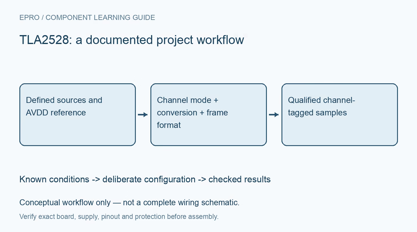
TLA2528 ADC: 7 Checks for Channel Identity and Averaged Data
TLA2528 checks for supply-referenced scaling, channel configuration, conversion timing, appended IDs and averaged-frame decoding. This is a documentation-based planning guide, not a report of independent hands-on testing.
1. Separate analog supply from digital-interface supply
The TLA2528 is an eight-channel twelve-bit ADC with an I2C interface and configurable digital pins. AVDD operates from 2.35 V to 5.5 V, while DVDD operates from 1.65 V to 5.5 V. AVDD also establishes the ADC reference; there is no independent external-reference pin to substitute casually. For an ordinary unaveraged result, the nominal code step is AVDD divided by 4096. Changes or noise on AVDD therefore affect voltage scaling and deserve an explicit measurement budget. Manufacturer documentation.
2. Configure each pin as analog or GPIO deliberately
The eight multifunction pins default to analog inputs after reset. Digital configuration requires distinguishing pin mode, GPIO direction, output-drive type and output value; these are not one interchangeable enable bit. When using an output, preload an appropriate latch value before enabling a load-facing drive path and verify the documented sequencing. Read back the configuration rather than trusting a software variable. Keep all analog sources within their allowed ranges and do not assume the digital-interface supply defines every multifunction pin behavior. Manufacturer documentation.
3. Budget source settling before scanning channels
The channels share a multiplexed conversion path rather than sampling eight sources simultaneously. Source resistance, switching capacitance and the ADC acquisition network can carry errors from a previous channel into the next result. Test a demanding transition between two different bounded input voltages, not only eight nearly identical sources. Choose any buffer, acquisition delay or discarded sample from the documented timing and source requirements. A correct channel-selection register alone does not demonstrate that the analog input has settled to the required accuracy. Manufacturer documentation.
4. Complete calibration and rebuild state after reset
The documented offset-calibration control clears when calibration has completed, so poll for completion rather than using an unexplained fixed delay. Offset calibration does not independently calibrate reference error or every gain error. A brownout or reset can invalidate prior pin and sequencing configuration; detect the relevant reset indication and rebuild the intended state. Address selection also depends on the documented reset-time behavior. Avoid borrowing statistics-register or calibration recipes from a related ADC whose register map is not the TLA2528 map. Manufacturer documentation.
Newest in the store


5. Associate read timing with the next conversion
In manual operation, channel selection and the read-trigger sequence must be interpreted together. The documented conversion initiation at the last-byte acknowledgement boundary means software must track which configuration produced each result, especially immediately after a channel change. Check the ninth falling SCL-edge behavior in the timing description rather than assuming the first returned word belongs to the newly selected input. The device can stretch the clock during conversion or averaging, so host timeout settings must accommodate legitimate activity without masking a stalled transaction. Manufacturer documentation.
6. Decode raw and averaged frame lengths separately
Without appended channel identification, a raw result occupies twelve significant bits in two bytes, with the unused lower nibble zero. Appending the four-bit channel ID uses that nibble. An averaged result can occupy sixteen bits; with an appended ID it requires three bytes, with the ID in the high nibble of the third byte. Configure and parse these formats as distinct records. A two-byte parser cannot silently consume an averaged-plus-ID stream without losing alignment or mislabeling channels. Manufacturer documentation.
7. Report averaging honestly and preserve sample identity
A sixteen-bit averaged output format does not transform the twelve-bit converter into a guaranteed sixteen-bit-accurate measurement system. Averaging can improve fractional resolution under appropriate noise conditions but costs time and does not remove correlated reference, settling or gain errors. Record channel ID, averaging setting, frame length, conversion state and supply-reference value alongside each voltage estimate. Validate the parser with known channel voltages and interrupted transfers. This produces a qualified channel-tagged record without claiming unsupported CRC protection or accuracy from the number of returned bits alone. Manufacturer documentation.
Related reading: ADS7038 ADC: 7 Checks for Channel Identity, Averaging and CRC.
Catalog note: The exact-part search did not return a matching Epro listing during preparation. Check the current catalog; this guide makes no price, availability or included-accessory claim.