


TMUX1308 Analog Multiplexer: 7 Checks for Reliable Channel Selection

TMUX1308 Analog Multiplexer: 7 Checks for Reliable Channel Selection
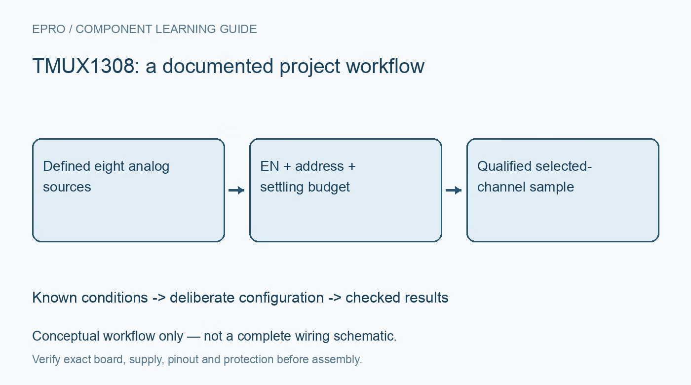
TMUX1308 checks for enable polarity, signal limits, injection-current control, ADC settling and fail-safe logic scope. This is a documentation-based planning guide, not a report of independent hands-on testing.
1. Separate the eight-channel mux from its relatives
The TMUX1308 is one eight-to-one bidirectional analog multiplexer; the related TMUX1309 has a different two-by-four channel arrangement. Confirm the exact part and package before drawing the pin map. The recommended supply range is 1.62 V to 5.5 V, and ordinary selected analog signals must remain between ground and VDD. This device neither amplifies the input nor provides galvanic isolation. Establish source ranges, ground relationships and transient exposure before connecting a sensor bank. Manufacturer documentation.
2. Use the active-low enable truth table
EN low connects the channel selected by A2:A0; EN high disconnects all channels. The address progresses from binary 000 for S0 through 111 for S7. Include the actual pin labels in firmware comments and verify each input with a distinct bounded test voltage. A reversed enable assumption can leave the output floating while software believes it is measuring a sensor. Define the startup address and enable state explicitly so reset behavior cannot select an unexpected source. Manufacturer documentation.
3. Limit fail-safe claims to the control inputs
The control inputs support 1.8 V-compatible logic under the documented operating conditions, including higher mux supply voltages. Their fail-safe behavior permits specified control levels before VDD is present. That feature concerns EN and the address pins; it does not give every analog terminal arbitrary power-off or overvoltage tolerance. Check control thresholds, leakage and sequencing from the relevant tables. Define unused controls at known levels and follow the manufacturer recommendation for grounding unused analog inputs in the final application. Manufacturer documentation.
4. Understand injection-current control without overpromising
Injection-current control helps prevent an out-of-range voltage on an unselected channel from disturbing the selected signal path. It is not a universal transient clamp and does not convert the selected path into a fault-protected input. The absence of a conventional diode path to VDD also does not remove every pin rating. Assess each possible fault against the recommended and absolute limits, adding suitable external protection when required. Start verification inside the normal signal range rather than demonstrating faults on an unprotected prototype. Manufacturer documentation.
Newest in the store


5. Account for resistance and source loading
The enabled path has finite on-resistance and signal-dependent behavior. Sensor source impedance, destination impedance and leakage therefore contribute to measurement error even when the channel number is correct. Calculate the divider effect for the actual load and consider leakage sensitivity for high-impedance sensors. A voltage observed with a high-impedance meter may not represent the value delivered into an ADC sampling network. Record the complete load condition rather than characterizing the mux as an ideal wire with no electrical consequences. Manufacturer documentation.
6. Budget settling after changing channels
Break-before-make operation avoids intentionally connecting two sources together during selection, but it does not guarantee an immediately accurate ADC result. Charge injection, path capacitance, source impedance and the converter acquisition network can retain part of the previous channel voltage. Apply a settling interval or discard a conversion only when justified by the actual converter timing. Test alternating low and high channel voltages as a demanding case. A fixed delay copied from another board is not evidence of settled data. Manufacturer documentation.
7. Preserve channel identity in the measurement record
Log the selected address, enable state, input source, supply, delay and ADC sample together. Confirm all eight mappings before adding an automated scan, then exercise controller resets and disabled intervals. Compare stable-channel readings with readings immediately following a large channel step. Keep source-fault containment and normal accuracy tests as distinct procedures. This produces a qualified channel-selection record without implying that injection-current control, fail-safe logic or a successful continuity check independently guarantees the accuracy of the final measurement system. Manufacturer documentation.
Related reading: TMUX1101 Analog Switch: 7 Checks for a High-Impedance Signal.
Catalog note: The exact-part search did not return a matching Epro listing during preparation. Check the current catalog; this guide makes no price, availability or included-accessory claim.