


TPS63031 Buck-Boost: 7 Checks for Fixed Output and Current Limits

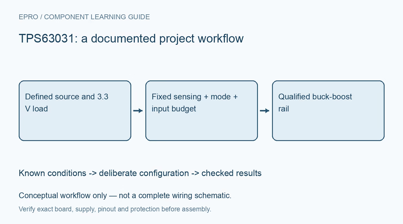
TPS63031 Buck-Boost: 7 Checks for Fixed Output and Current Limits
Plan a TPS63031 fixed 3.3 V buck-boost supply with correct FB sensing, input-dependent load capability, mode control and realistic shutdown expectations. This is a documentation-based planning guide, not a report of independent hands-on testing.
1. Confirm the fixed-output member before using a divider
TPS63031 is the fixed 3.3 V member of the TPS6303x family, while TPS63030 is adjustable. The fixed part uses FB to sense its output and requires the documented direct connection to VOUT. Copying the adjustable member resistor divider changes that intended sensing arrangement. Verify the package marking, bill of materials and schematic together before powering a board. A regulator family title describing adjustable options does not mean every orderable member accepts the same feedback network. Manufacturer documentation.
2. Build the source budget across buck and boost regions
The converter can operate with input voltage above or below the regulated output, but available output current depends on the operating point. At low input voltage, supplying the same output power requires more input current after accounting for efficiency. Include source resistance, connectors and battery droop in the budget. The 1 A switch headline is not a guaranteed 1 A output rating. Use the documented load curves and operating conditions rather than one current figure for the entire source range. Manufacturer documentation.
3. Select the inductor and capacitors for actual switching stress
Check the recommended component range, inductor saturation current and winding loss under the worst input condition. Output-capacitor effective capacitance can be lower than its label after DC bias, tolerance and temperature are included. Keep the power loop compact and place the required input and analog-supply bypassing near the device. A breadboard-style long switching loop can defeat an otherwise reasonable schematic. The exposed pad and ground layout are part of the electrical and thermal implementation, not optional mechanical details. Manufacturer documentation.
4. Define the PS/SYNC policy instead of leaving it ambiguous
PS/SYNC controls the documented power-save or fixed-frequency behavior and can support synchronization under specified conditions. Choose a deterministic connection consistent with the desired operating mode and the host power sequence. Light-load power saving can change ripple and switching patterns without indicating a failed converter. Conversely, forced switching can increase light-load consumption. Compare rail noise and source current in the mode actually intended for the application, rather than selecting a mode solely because a scope trace looks more regular. Manufacturer documentation.
Newest in the store


5. Observe crossover under a bounded load
Sweep a current-limited source through input values below, near and above 3.3 V while keeping the load inside the verified operating envelope. Record input current, output voltage and transient behavior at each point. Start conservatively and stop if the source collapses or thermal limits are approached. Crossover regulation is a system behavior involving source impedance and layout, not just a topology label. Do not conclude that a no-load sweep establishes maximum usable load at the lowest input voltage. Manufacturer documentation.
6. Verify disable behavior without promising instant discharge
The datasheet describes load disconnect during shutdown, which is useful for limiting battery drain through the converter. That does not by itself define how quickly an externally charged output capacitor reaches a safe voltage. Measure the actual load-side decay and consider other circuits that can feed the output. Review pin limits during input removal and externally powered conditions. If downstream logic needs a guaranteed reset interval or discharge time, design that requirement explicitly rather than relying on an unspecified parasitic path. Manufacturer documentation.
7. Preserve an operating envelope with the finished design
Record the fixed part number, feedback connection, component values, PS/SYNC state, source range and accepted load profile. Include startup with a discharged output, load steps and repeated enable cycles. Compare the worst observed temperatures and voltage excursions with the manufacturer limits and the load requirements. Do not turn a typical efficiency curve into a guaranteed battery-life claim. This documentation-based review provides a structured plan; the final board current rating and noise performance require measurements under its real operating conditions. Manufacturer documentation.
Related reading: TPS63070 Buck-Boost: 7 Checks Across the Input-Output Boundary.
Catalog note: The exact-part search did not return a matching Epro listing during preparation. Check the current catalog; this guide makes no price, availability or included-accessory claim.