


UCC27531 Gate Driver: 7 Checks for Split Outputs and Package-Dependent Enable

UCC27531 Gate Driver: 7 Checks for Split Outputs and Package-Dependent Enable
Review UCC27531 package differences, split gate resistors, enable behavior, supply limits and realistic gate-drive power. This is a documentation-based planning guide, not a report of independent hands-on testing.
1. Read the package suffix before wiring
The UCC27531 name alone does not fully specify the interface. The DBV version uses separate OUTH and OUTL connections plus EN, while the documented D version has a single output and is always enabled. Confirm the complete ordering code, top-view pinout and board routing before adapting a schematic. A pad bearing the same location on another family member need not provide the same function. Save the exact package identity in the project record. Manufacturer documentation.
2. Match the supply to the power switch
The recommended driver supply range is 10V to 35V. That range describes the driver, not a promise that the connected MOSFET or IGBT gate can tolerate 35V. Select the rail using the power-switch gate rating and required enhancement voltage, including tolerance and ringing. A higher supply can increase switching speed while increasing gate stress and drive loss. Keep a small, protected bench supply for initial testing and review undervoltage-lockout behavior before applying a power-stage bus. Manufacturer documentation.
3. Define input and enable states
For the DBV device, a high IN produces a high combined output only when the driver is enabled. EN low commands the gate low; an unconnected EN can leave the device enabled according to the truth table. Do not use a floating enable as a safety interlock. Provide deliberate reset-time states and verify their logic thresholds. The D package cannot substitute its missing enable with software expectations; shutdown must be implemented elsewhere in a suitably reviewed design. Manufacturer documentation.
4. Use split outputs for separate edge control
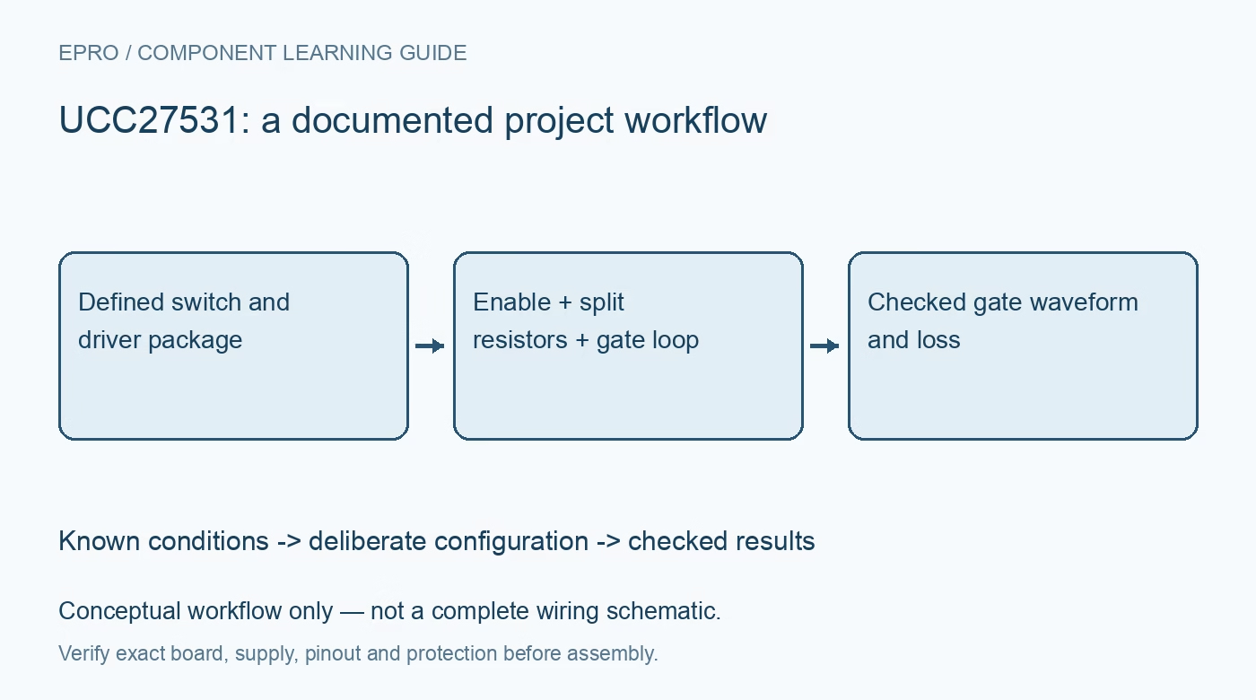
OUTH supplies gate charging current and OUTL removes gate charge. The split-output version allows different turn-on and turn-off resistances, with both paths meeting at the switch gate. Trace the actual connections before changing resistor values: the pins are complementary drive paths, not independent logic channels. Start with conservative edge rates and inspect both transitions. Faster turn-off may improve one condition while increasing ringing or ground disturbance elsewhere, so qualify the complete gate loop rather than a resistor in isolation. Manufacturer documentation.
Newest in the store


5. Interpret peak current as a transient capability
The headline drive capability is approximately 2.5A sourcing and 5A sinking under specified conditions, not continuous output current available to a load. Estimate average gate-charge demand from Qg multiplied by switching frequency, and approximate gate-drive energy from Qg times drive voltage per cycle. These are planning calculations, not a complete driver dissipation model. Include switching frequency, gate charge at the actual operating point and external resistance when comparing designs. Recheck package temperature at the intended repetitive operating condition. Manufacturer documentation.
6. Keep the reference and gate loop controlled
Place local bypassing close to the driver supply and ground pins and keep the gate-current loop compact. Input tolerance to negative voltage does not make arbitrary ground bounce harmless to the controller or power switch. Measure the gate relative to its source or emitter using an appropriate probing method; long probe ground leads can create misleading ringing. This is not an isolated driver. Any floating high-side application requires a separately justified bias and signal-isolation arrangement, not a direct ground-referenced shortcut. Manufacturer documentation.
7. Test shutdown before energetic switching
Begin with a representative low-energy capacitive gate load and verify polarity, enable action and supply recovery. Move to the actual switch only after the control behavior is understood, keeping the power-stage energy bounded. Check gate overshoot, undershoot, off-state voltage and driver temperature across the intended operating cases. Keep mains and high-energy buses out of a beginner bench procedure. Record the package, rail, resistor values, load and probe arrangement so later waveform comparisons refer to the same configuration. Manufacturer documentation.
Related reading: UCC27624 Gate Driver: 7 Checks for Negative Inputs and Transient Output Limits.
Catalog note: The exact-part search did not return a matching Epro listing during preparation. Check the current catalog; this guide makes no price, availability or included-accessory claim.