


MCP3008 ADC: Reference Voltage, Eight Channels and SPI Selection

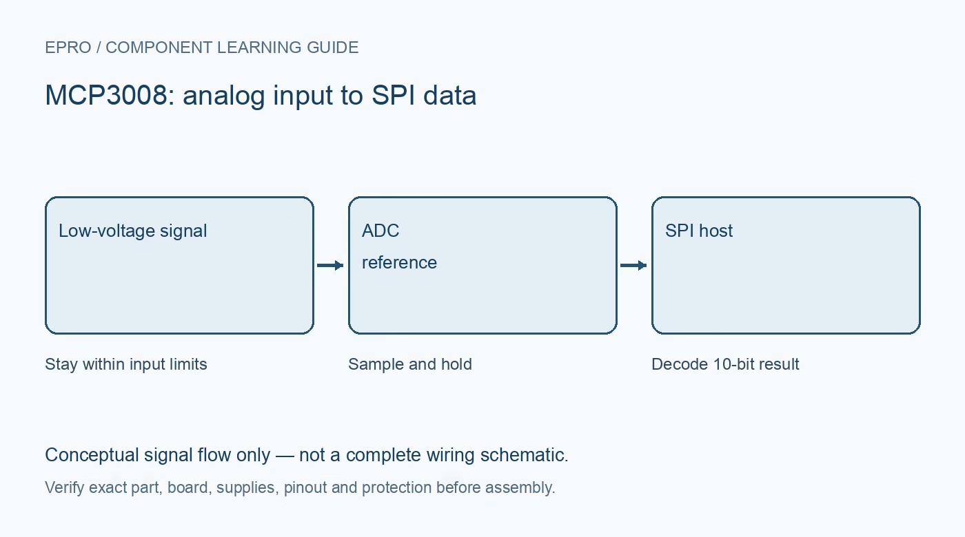
The MCP3008 adds eight multiplexed analog inputs through an SPI interface. Its 10-bit result is useful only when the input range, reference voltage, source impedance and host logic are chosen together. An extra ADC channel is not automatic permission to measure an arbitrary voltage.
Separate resolution from accuracy
Ten bits provide 1024 ideal quantization steps, not an assurance that every measurement is accurate to one part in 1024. Reference error, input noise, linearity, grounding and source loading influence the actual result. Keep raw conversion counts available while developing the circuit so a scaling error is not hidden behind a formatted voltage display.
Choose supply and reference together
The referenced datasheet specifies 2.7–5.5 V operation and explains how VREF sets the conversion scale. A common 3.3 V host design can use a compatible 3.3 V ADC supply and reference, subject to the complete electrical requirements. Do not power the ADC at 5 V and assume its output or logic thresholds are automatically suitable for a 3.3 V host.
Understand the multiplexed channel arrangement
MCP3008 provides eight input channels with single-ended and pseudo-differential configurations. It is not eight simultaneous sample-and-hold channels, and pseudo-differential operation is not permission for arbitrary negative input voltage. Choose the documented mode and obey absolute input limits for every terminal.
Check sampling time and source impedance
The ADC samples onto an internal capacitor for a limited acquisition interval. A high-impedance sensor or large series resistance may not charge that capacitor accurately at the selected clock. Follow the datasheet input model and buffering guidance rather than assuming slower application printing solves acquisition errors. Filtering must also be designed for the actual signal bandwidth.
Plan the SPI transaction and bus
The host supplies clock, command data and chip select; the ADC returns serial data. Use a driver that handles the start bit, channel configuration, null bit and ten result bits correctly. Observe clock limits for the chosen supply and keep transactions within the documented timing. Separate chip selects are required when sharing a suitable bus with other devices.
Choose documentation over a claimed sample-rate headline
The maximum conversion rate depends on supply and timing conditions, and a software library may run much slower. Budget for reference quality, wiring, signal conditioning and measurement validation rather than buying only by channel count. This is an educational low-voltage ADC; mains, battery-pack and industrial measurements require appropriate engineered front ends and isolation where needed.Newest in the store


Availability and illustration note
No matching product was found in the checked Epro catalog for this topic on 19 October 2026. This article therefore does not quote an Epro price or claim stock. The original illustration shows conceptual signal flow only, not a complete circuit or a photograph of a supplied product. Obtain a documented component or carrier with a known pinout and electrical specification.
Frequently asked questions
Can MCP3008 directly read any voltage below 5 V?
No. Input limits depend on the chosen supply, reference and configuration, and must be checked before connection.
Does 10-bit resolution mean 10-bit absolute accuracy?
No. Reference, converter errors, noise and circuit design affect accuracy as well as resolution.
Related Epro reading
Review breadboard connections before assembling a prototype. For controller expansion, the Mega 2560 pin guide explains why pin names and electrical limits must be checked together.
Technical references and test limitations
This guide uses the documentation linked below. The procedures are for a controlled, low-voltage learning setup; no independent hands-on test of the particular seller board is claimed. Record the actual part markings, wiring and firmware version before drawing conclusions from a test.