


74HC14 Schmitt Trigger: 7 Hysteresis and Input Checks

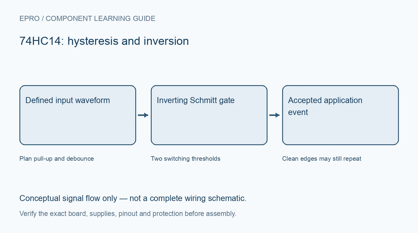
A 74HC14 contains six inverting Schmitt-trigger gates. Hysteresis helps turn a slowly changing voltage into a defined digital transition, but it does not make every noisy input or bouncing switch produce one event. Design the signal-conditioning network and logic interpretation together.
Identify HC and HCT correctly
The cited family document covers variants with different input-level requirements. A 74HCT14 is not simply the same device with an extra letter for packaging. Verify the actual fitted manufacturer and suffix before relying on a particular threshold or supply assumption.
Understand the two switching thresholds
A rising input crosses a positive-going threshold, while a falling input crosses a lower negative-going threshold. The difference is hysteresis. These thresholds vary within specified limits, so an RC timing calculation must not treat one typical threshold as an exact precision reference.
Account for the inversion
A sufficiently low input produces a high output and a sufficiently high input produces a low output. That polarity matters for active-low buttons and edge-triggered counters. If two gates are used to restore polarity, include both stages in the timing and startup analysis.
Do not confuse clean edges with debounce
A mechanical switch can create several genuine threshold crossings during one press. Schmitt action sharpens those transitions but may preserve multiple events. Use an appropriate RC network or another debounce strategy and validate both press and release under representative contact behaviour.
Keep input voltage within operating limits
A Schmitt input is not a universal overvoltage-tolerant input or a mains interface. Check the recommended rail limits and any required protection for the exact part. Do not apply a negative, oversized or unrelated supply signal merely because a diagram shows an input resistor.
Define unused inputs and loading
Tie unused gate inputs to valid logic levels as documented and leave unused outputs free. Add local decoupling. Output drive is limited; use suitable resistors or a separate driver for loads rather than treating a clean digital edge as permission to drive a relay coil.
Newest in the store


Treat oscillator timing as approximate
RC oscillator or pulse-shaping demonstrations depend on component tolerance, thresholds, supply and loading. They can be useful learning circuits without being precision timebases. Validate the complete design before relying on it for event counting, communication timing or any protection-related function.
Frequently asked questions
Will one Schmitt gate always remove switch bounce?
No. Multiple real threshold crossings can still create multiple output edges.
Does the output follow the input polarity?
No. A 74HC14 is inverting; include that polarity in the surrounding logic design.
Availability and illustration note
No matching Epro product was returned by the catalog search on 21 October 2026 UTC. This learning guide does not assert stock, a selling price or compatibility of an unidentified substitute. The illustration is an original conceptual signal-flow diagram, not a product photograph or complete wiring schematic.
Related Epro reading
For a first bench setup, review breadboard connections and continuity checks and I2C voltage-level translation. These guides do not replace the exact module schematic.
Technical references and limitations
Source: Nexperia 74HC14/74HCT14 datasheet. Electrical limits apply to the named part, not automatically to every carrier board. This is a documentation-based learning workflow, not a claim of independent hardware testing, traceable calibration or safety certification.