


ADS1118 ADC: 7 Checks for SPI, Input Range and Temperature Mode

ADS1118 ADC: 7 Checks for SPI, Input Range and Temperature Mode
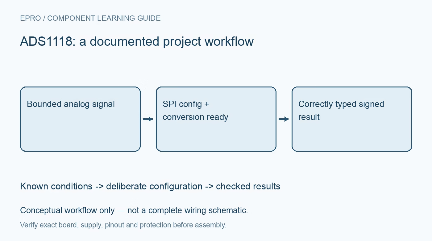
Use ADS1118 SPI conversions with verified configuration, bounded analog inputs and distinct decoding for ADC and internal temperature results. This is a documentation-based project guide, not an independent hands-on test report.
1. Distinguish ADS1118 from I2C relatives
ADS1118 is a sixteen-bit delta-sigma ADC with an SPI-compatible interface, internal reference and internal temperature sensor. Texas Instruments documents differential and single-ended input selections. Despite similar naming, an ADS1115 wiring diagram or library is not automatically suitable. Write down the exact converter, board revision and required signal range. This article separates communication, analog validity and numerical decoding so that one successful register transfer cannot stand in for all three. Manufacturer documentation.
2. Check every analog pin against the rails
Choose a PGA full-scale range for the differential signal, but independently verify each input voltage against the permitted supply-relative limits. Selecting a range larger than the supply does not allow an input pin to exceed its electrical limits. Consider source impedance, filtering and any possible fault voltage. Start with a bounded low-voltage source and no connection to mains or an unknown external circuit. Differential measurement does not provide isolation. Manufacturer documentation.
3. Verify SPI edges and configuration bits
Configure the host from the documented serial timing; the datasheet application guidance uses SPI mode 1. Check chip select, clock, input and output signals against the carrier labels. Preserve the required configuration-bit values and confirm configuration read-back when using the supported transaction format. A generic sixteen-clock read may not perform the intended configuration update. Keep a raw transaction capture or logic-analyzer trace during bring-up if behavior is inconsistent. Manufacturer documentation.
4. Wait for the conversion you requested
In single-shot mode, start a new conversion through the documented control sequence and then wait for completion. Distinguish the prior buffered result from the newly requested measurement. DOUT/DRDY behavior depends on chip-select state, so an inactive shared-bus device cannot always signal readiness the way a permanently selected one does. Use a bounded timeout and preserve channel, mode and timing context when accepting a result after a configuration change. Manufacturer documentation.
Newest in the store


5. Decode ADC and temperature results differently
The ADC voltage result and internal temperature result are different formats. Apply the correct signed interpretation, bit alignment and scale for the selected mode. Do not run both through the same voltage conversion helper. The internal temperature sensor measures the local device thermal condition, not a remote object. If using it within thermocouple compensation, the connector thermal design, thermocouple type and transfer calculation remain separate engineering requirements. Manufacturer documentation.
6. Prove the channel and range mapping
Apply several known bounded voltages and verify which configured input pair each result represents. Compare a differential zero with a small positive signal, and test a negative differential only within the safe per-pin limits. Check units before plotting: raw counts, volts and millivolts should have explicit labels. Multiplexer switching and data-rate choices belong in the test record so a stale sample is not misidentified as the new channel. Manufacturer documentation.
7. Keep ADS1118 validity with each sample
Save configuration read-back, raw conversion, mode, selected inputs, PGA range, readiness outcome and timestamp. Record timeouts without converting them into a plausible zero. Compare the result with a suitable reference and include source and meter uncertainty when judging error. The related ADS1115 guide provides ADC selection background but uses a different interface. ADS1118 success means a fresh, electrically valid, correctly decoded result, not merely a responsive SPI bus. Manufacturer documentation.
Related reading: ADS1115 ADC: 7 Checks Before Buying.
Catalog note: The exact-part search did not return a matching Epro listing during preparation. Check the current catalog; this guide makes no availability, price or accessory claim.