


ADS8332 Multiplexed ADC: 7 Checks for Acquisition and Channel Tags

ADS8332 Multiplexed ADC: 7 Checks for Acquisition and Channel Tags
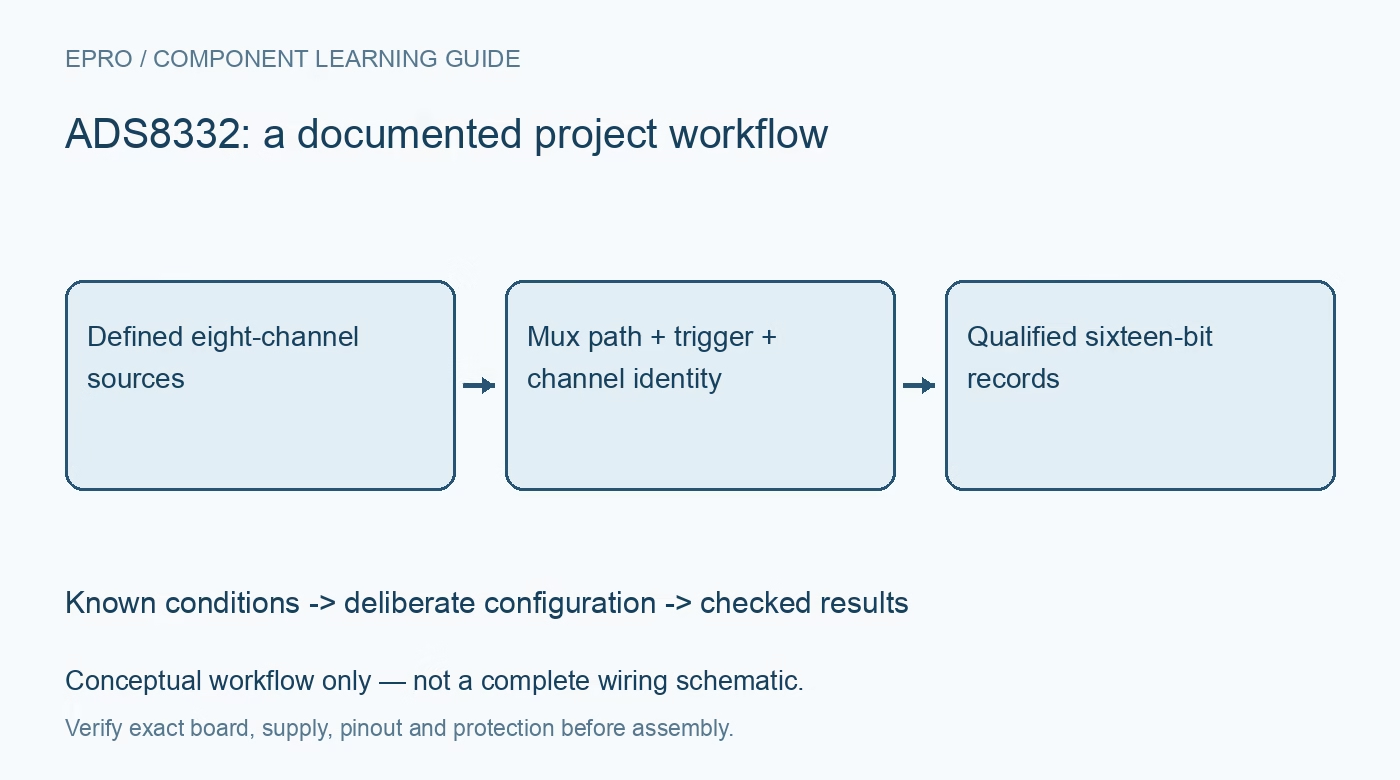
Plan ADS8332 acquisition with the exposed mux-to-ADC path, conversion triggering, reference drive and channel identification matched to the selected mode. This is a documentation-based planning guide, not a report of independent hands-on testing.
1. Define eight inputs as a multiplexed system
ADS8332 combines an eight-channel multiplexer with a sixteen-bit SAR converter. It does not sample all eight channels simultaneously. Specify the required per-channel rate, scan order and permitted time skew before quoting the headline total sampling rate. Check each signal relative to the shared COM input, reference and analog supply limits. Low-voltage protected sources belong in the initial test setup; the presence of a COM terminal does not make the converter an isolated input or permit unrestricted common-mode voltage. Manufacturer documentation.
2. Complete the exposed MUXOUT-to-ADCIN signal path
The manufacturer exposes the multiplexer output and ADC input so shared conditioning can be placed between them. The path must be connected according to the chosen circuit, not left open because the chip contains an internal mux. If a buffer, filter or programmable amplifier is inserted, its gain, settling and headroom become part of every channel measurement. Verify pin numbers against the exact package. A working SPI interface cannot compensate for a missing or incorrectly biased analog connection between these terminals. Manufacturer documentation.
3. Budget acquisition for the worst channel transition
A transition from one channel near the low end of range to another near the high end can be more demanding than repeatedly sampling a steady voltage. The SAR input draws charge during acquisition, and the shared conditioning path must settle to the required error band. Include source impedance, mux behavior, filter resistance and amplifier recovery. A large smoothing capacitor may improve a static trace while slowing channel changes. Test alternating extreme channels rather than validating only consecutive samples from the same source. Manufacturer documentation.
4. Choose manual or automatic channel control explicitly
The configuration register selects channel-control behavior, while manual operation uses the command register to request the intended input. Automatic scanning follows its documented sequence. Keep channel changes, acquisition and conversion start in the correct order for that mode. Do not label a returned word solely with the last command sent by the host. Preserve a clear record of which input was acquired for each conversion and how the driver establishes that association after reset or an interrupted transfer. Manufacturer documentation.
Newest in the store


5. Coordinate CONVST, conversion clock and serial readout
The converter supports a conversion-start function independent of chip select and a choice of conversion-clock source. Select the documented trigger and timing arrangement rather than assuming every CS edge creates a new sample. If the serial clock also participates in conversion timing, its requirements affect acquisition scheduling as well as data transfer. Configure EOC or interrupt behavior consistently and budget the complete readout. Missed deadlines should be reported as acquisition faults, not replaced silently by the preceding word. Manufacturer documentation.
6. Preserve reference and channel metadata beside raw codes
Use an external reference with the documented bypassing and dynamic drive capability, and include reference error in the voltage scale. If channel tagging is enabled, decode the complete documented output format rather than treating every received bit as conversion data. Keep the tag, scan configuration, reference value and timestamp together. Tags support data attribution, but do not prove the external source or conditioning stage has settled. Test parser alignment with distinct known voltages so swapped channels cannot hide behind similar readings. Manufacturer documentation.
7. Validate restart and scan coherence before final integration
Begin with bounded inputs, then test channel alternation, manual selection, automatic scanning and reset recovery using a saved register snapshot. Compare raw frames with predicted reference-based values and verify that each record retains the correct channel identity. Repeat at the intended aggregate rate and with realistic source impedances. Document the conditioning network and timing margins. This manufacturer-based guide supplies a validation plan, not independent linearity, noise or simultaneous-sampling performance claims for an untested board. Manufacturer documentation.
Related reading: ADS7953 Multiplexed ADC: 7 Checks for Channel Frames and Range.
Catalog note: The exact-part search did not return a matching Epro listing during preparation. Check the current catalog; this guide makes no price, availability or included-accessory claim.