


TPS22917 Load Switch: 7 Checks for Reverse Blocking and Timing

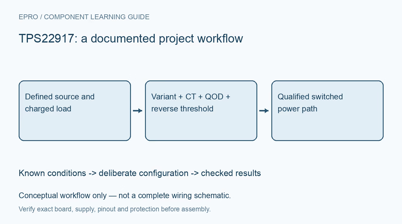
TPS22917 Load Switch: 7 Checks for Reverse Blocking and Timing
Review TPS22917 switching with threshold-based reverse-current blocking, CT rise control, QOD discharge and the correct active-high or active-low variant. This is a documentation-based planning guide, not a report of independent hands-on testing.
1. Confirm enable polarity from the exact variant
TPS22917 uses active-high control, while TPS22917L uses active-low logic. Verify the orderable device, pinout and intended default state before connecting the host. The family operates from 1 V to 5.5 V and supports its documented current envelope with appropriate thermal design. It is a load switch, not a voltage regulator. A generic schematic label ending only in the family name is insufficient if firmware assumes the opposite ON polarity or the host resets into an uncontrolled level. Manufacturer documentation.
2. Calculate conduction loss at the actual input voltage
On-resistance varies with supply voltage and temperature, so the lowest headline resistance does not apply everywhere. Estimate output droop and dissipation at the maximum sustained load, then check package and board cooling. Include connectors and copper in the load path. The current headline is not a programmable output-current limit. If the system needs precision current regulation or additional fault telemetry, provide suitable external circuitry or choose a device with those explicitly documented capabilities. Manufacturer documentation.
3. Use CT to shape inrush rather than promise a hard limit
The timing capacitor controls output rise behavior and can reduce the charging current of load capacitance. Approximate capacitor charging current from capacitance and voltage slew, then add any active load current during the ramp. Use the documented timing curves to select a starting value and measure the finished board. A slow ramp can still draw substantial current if downstream circuits activate before regulation. Check the input source current-limit behavior rather than treating CT as an exact electronic fuse setting. Manufacturer documentation.
4. Choose QOD for the required fall-time behavior
QOD provides an adjustable discharge path when used according to the application circuit. The documented options include connecting it directly or through resistance to the output, while leaving it open produces a slower discharge governed by other paths. Check capacitor energy, pulse dissipation and the load reset requirement. A discharge time quoted for one capacitance and resistor does not apply to every assembly. Do not connect QOD as though it were an ordinary permanent ground pin or assume the output becomes zero immediately after disable. Manufacturer documentation.
Newest in the store


5. Understand the threshold and delay in reverse blocking
The full-time reverse-current-blocking feature detects the documented reverse-current condition and disables the switch after its response time. It is not an ideal diode that permits absolutely no reverse charge under every transient. The datasheet describes automatic restart with slew control after the reverse condition clears. Review threshold, delay and permitted pin conditions for a precharged or externally supplied output. Avoid assuming that a weak upstream source can tolerate any reverse pulse simply because reverse blocking appears in the feature list. Manufacturer documentation.
6. Include smart-control and partial-power conditions
The ON control includes a smart bias arrangement to reduce unnecessary static current, but the exact active-high or active-low variant still governs the intended behavior. Follow its documented control guidance during host startup, reset and loss of power. Evaluate a charged output with VIN absent separately from ordinary enable switching. Identify every possible source feeding the load node, including communications pins from another board. Reverse-current blocking on the power path does not isolate all signal paths or eliminate system-level backfeeding. Manufacturer documentation.
7. Validate forward, disable and reverse transitions safely
Use current-limited low-voltage sources and noncritical loads to measure the rise, fall, conduction drop and selected reverse-condition response within ratings. Capture input and output behavior rather than checking only the final voltage. Exercise repeated transitions with partly discharged capacitors and verify that automatic restart cannot create an unsafe sequence. Save device variant, CT, QOD network, source settings and load capacitance. This is manufacturer-based planning guidance, not independent reverse-leakage, inrush-limit or thermal validation of an assembled design. Manufacturer documentation.
Related reading: TPS22918 Load Switch: 7 Checks for an Orderly Sensor Rail.
Catalog note: The exact-part search did not return a matching Epro listing during preparation. Check the current catalog; this guide makes no price, availability or included-accessory claim.