


TPS22924C Load Switch: 7 Checks for Slow Rise and Residual Voltage

TPS22924C Load Switch: 7 Checks for Slow Rise and Residual Voltage
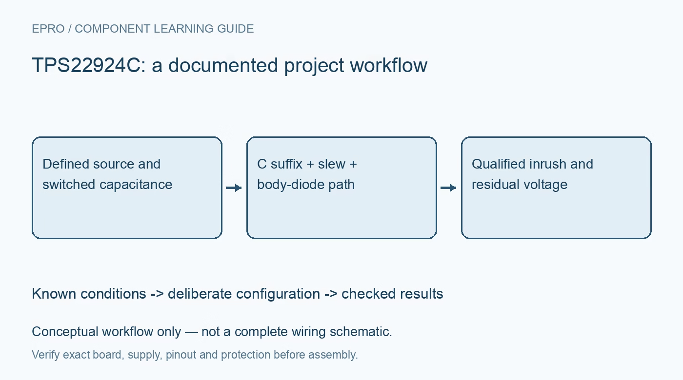
Plan TPS22924C switching with seven checks for the 3.6-V ceiling, C-suffix rise time, inrush, body-diode paths and self-disconnecting discharge. This is a documentation-based planning guide, not a report of independent hands-on testing.
1. Identify the C suffix and its intended voltage range
TPS22924C is a controlled-turn-on NMOS load switch for a recommended input range of 0.75 V to 3.6 V. It is not a direct 5-V USB power switch. The family includes a B version with substantially different rise time, so check the complete order code and six-ball package drawing. A small assembled module may include other components, but do not assume they extend the IC ratings or provide protection absent from its documented circuit. Manufacturer documentation.
2. Define ON and the off state before applying power
The ON control is active high and accepts documented low-voltage logic levels. Provide a defined inactive condition during processor reset and supply sequencing instead of leaving ON floating. Verify thresholds at the intended VIN and confirm that the host cannot back-power the unpowered switch through a control connection. During early tests, use a benign resistor load and observe VIN, ON and VOUT together. The software command alone cannot show whether the actual rail has reached a safe state. Manufacturer documentation.
3. Use the C rise time, not the faster B figure
At VIN of 3.6 V, the datasheet describes a typical rise time of 800 microseconds for TPS22924C, versus 100 microseconds for TPS22924B. These are condition-dependent figures, not guaranteed timing at every voltage and load. Estimate the capacitive charging current from capacitance multiplied by rail change divided by ramp duration, then include the downstream operating current. Check measured source droop and peak current because real rail ramps and dynamic loads are not ideal straight lines. Manufacturer documentation.
4. Preserve margin in current and conduction loss
The headline 2-A maximum continuous switch current is not an unconditional board rating. On-resistance depends on input voltage and temperature, and the resulting heat approximately follows current squared multiplied by resistance. Include package thermal behavior, copper routing, connector capacity and repetitive startup energy in the design. Do not describe controlled slew as programmable current regulation: the datasheet does not establish a general-purpose adjustable current limiter. Use an appropriately limited upstream source during development and provide the protection the system actually requires. Manufacturer documentation.
Newest in the store


5. Recognize that output discharge stops before zero
An on-chip discharge path is enabled when the main pass transistor is turned off. The important detail is that the pulldown automatically disconnects when output reaches approximately ten percent of the rail, minimizing shutdown current. Consequently, an off command does not guarantee a zero-volt output or full reset of a high-impedance peripheral. Measure residual voltage after the expected off interval. Add a properly analyzed external discharge path if the application needs a lower, timed reset threshold. Manufacturer documentation.
6. Analyze the body diode and every alternate supply path
The datasheet warns that output capacitance exceeding input capacitance can make VOUT rise above VIN when input power is removed, allowing current through the intrinsic body diode. A ten-to-one CIN-to-load-capacitance ratio is recommended for minimizing startup input dip, but that recommendation is not a reverse-current blocker. Review live signal pins, debug cables and other rails that can feed the switched domain. Do not promise isolation between supplies merely because the main transistor has been commanded off. Manufacturer documentation.
7. Validate both the first and repeated power cycles
Capture a cold start, an ordinary disable, input removal and repeated short off intervals using a current-limited source and noncritical load. Compare the lowest measured VOUT with the peripheral reset requirement, not just an LED turning dark. Record capacitances, VIN, load, control levels and scope timing. Check that source recovery and residual charge do not accumulate across cycles. The successful result is a bounded startup-and-reset sequence for the tested conditions, not a blanket claim that any attached device will restart. Manufacturer documentation.
Related reading: TPS22922 Load Switch: 7 Checks for Discharge and Inrush.
Catalog note: The exact-part search did not return a matching Epro listing during preparation. Check the current catalog; this guide makes no price, availability or included-accessory claim.