


SN74AHCT125 Buffer: 7 Checks for 3.3-V to 5-V Signals

SN74AHCT125 Buffer: 7 Checks for 3.3-V to 5-V Signals
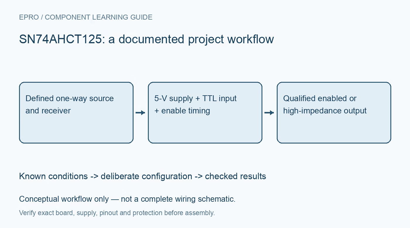
Plan SN74AHCT125 interfaces with seven checks for TTL input thresholds, active-low enables, output contention, edge rates and power sequencing. This is a documentation-based planning guide, not a report of independent hands-on testing.
1. Use the AHCT supply range rather than a family guess
SN74AHCT125 contains four noninverting buffers with independent three-state output controls. Its recommended supply range is 4.5 V to 5.5 V, not 3.3 V simply because the signal source is a 3.3-V processor. The AHCT input thresholds are TTL-compatible. Confirm the complete part marking and package pinout; a nearby HC, AHC or LVC device may have different thresholds and supply requirements. A breadboard label that says 125 does not establish which electrical family is installed. Manufacturer documentation.
2. Check guaranteed thresholds in both directions
The recommended input high threshold is 2 V and input low threshold is 0.8 V. A 3.3-V source can therefore be suitable when its guaranteed high and low outputs meet these levels under the actual load. The buffer output, however, is driven from its approximately 5-V supply. It must not be sent into an unprotected 3.3-V-only receiver. This is a one-way interface arrangement, not automatic bidirectional translation; verify every signal direction and receiving absolute limit independently. Manufacturer documentation.
3. Define output enable before the processor starts
Each active-low OE enables its corresponding A-to-Y path when low. A high OE places Y in a high-impedance state; it does not force Y to logic zero. The manufacturer recommends pulling OE toward VCC to favor a disabled output during power-up and power-down. Size that resistor for the controlling device and review whether a low-voltage host tolerates the pull-up voltage. An open-drain or separate control stage may be needed rather than directly exposing a processor pin to 5 V. Manufacturer documentation.
4. Prevent contention when outputs share a conductor
A three-state output can share a bus only when the system guarantees that incompatible drivers are not enabled together. Include disable and enable propagation times and any skew when changing ownership. Do not join two active push-pull outputs and expect the stronger one to win safely. During development, observe ownership changes with a benign load and capture OE alongside data. If the receiving node must retain a defined level when every driver is disabled, provide a correctly analyzed external bias. Manufacturer documentation.
Newest in the store




5. Do not treat the buffer as a Schmitt-trigger debounce circuit
The device is not specified as a Schmitt-trigger input buffer. Its recommended input transition requirement is 20 nanoseconds per volt, so a slowly rising RC node or bouncing mechanical switch is not automatically a valid clean input. An ordinary buffer can reproduce glitches rather than remove them. Use a suitable Schmitt input, comparator or explicit debounce strategy where needed, and then verify the resulting edge rate and logic levels. Avoid repeating broad application-list language as a guarantee of noise cleanup. Manufacturer documentation.
6. Budget load current, capacitance and return paths
The recommended static output drive is specified separately from absolute-maximum pin and package current. Absolute-maximum values are not a continuous operating target, and this buffer is not a general-purpose LED-strip power driver. Capacitive loads, long wiring and multiple receiving inputs affect edge shape and supply transients. Fit local bypassing, keep return paths short and measure at the receiver. Use source termination where a reviewed interconnect design calls for it, rather than adding an arbitrary resistor without checking timing margin. Manufacturer documentation.
7. Validate powered and unpowered combinations
Tie unused data and enable inputs to defined valid levels even if their outputs are not used. Test normal operation, disabled high impedance, host reset and each relevant supply-order combination without exceeding input or output limits. Do not assume partial-power-down isolation or fail-safe behavior that has not been established for this exact part. Record supply, source levels, receiving tolerance, OE state and measured timing. A reliable interface is one with verified logic margins and sequencing, not merely a waveform that looks taller on an oscilloscope. Manufacturer documentation.
Related reading: SN74LVC1T45 Translator: 7 Checks for Direction and Power States.
Catalog note: The exact-part search did not return a matching Epro listing during preparation. Check the current catalog; this guide makes no price, availability or included-accessory claim.