


UCC27524A Gate Driver: 7 Checks for Dual-Channel Timing and Enable States

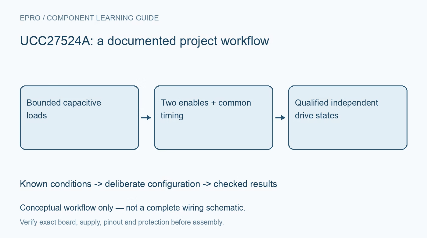
UCC27524A Gate Driver: 7 Checks for Dual-Channel Timing and Enable States
Check UCC27524A dual gate-drive timing, default enable behavior, peak-current limits and the conditions needed before paralleling outputs. This is a documentation-based planning guide, not a report of independent hands-on testing.
1. Define two low-side channels before selecting a load
The UCC27524A contains two noninverting low-side gate-driver channels operating from a 4.5-to-18-volt supply. It is not an isolated driver or a high-side level shifter. Define the gate-source voltage required by each transistor and the reference shared with the controller. For initial checks, disconnect the power stage and use benign capacitive gate-equivalent loads with a current-limited low-voltage supply. A valid logic waveform alone does not establish a safe switching-power topology or adequate transistor protection. Manufacturer documentation.
2. Distinguish enabled-by-default from fail-safe disabled
ENA and ENB are active-high enables with internal pullups. Leaving an enable floating therefore does not deliberately inhibit its channel. By contrast, floating main inputs are arranged to hold the corresponding outputs low, and undervoltage lockout also holds outputs low. These are different mechanisms. Specify enable and command levels during controller reset, programming and supply ramping. Verify the actual pull network rather than assuming the word enable means an unconnected pin automatically provides a safe off state. Manufacturer documentation.
3. Use fixed input thresholds, not a supply-ratio guess
The logic inputs use TTL/CMOS-compatible thresholds that are independent of the gate-drive supply. Compare guaranteed controller levels against the driver threshold table over the intended conditions. Do not reuse a supply-proportional CMOS threshold calculation from a different driver. Review input undershoot, overshoot and pin-specific ratings separately; a headline about negative-input robustness is not permission to apply arbitrary negative voltage to every control terminal. Measure logic at the driver reference, where return-path noise actually appears. Manufacturer documentation.
4. Convert peak output current into a gate-charge budget
The five-amp source and sink figures describe peak drive capability into capacitive loads, not a continuous five-amp supply for an external device. Estimate average gate-drive demand from total gate charge and switching frequency, then account for losses and both channels. Gate resistors influence edge speed, ringing and driver dissipation. Keep local bypassing and current loops compact. Confirm the chosen transistor gate limits and output loading before using the fastest possible transition as a design target. Manufacturer documentation.
Newest in the store


5. Treat matched delay as finite, not an interlock
TI specifies closely matched channel propagation delays, but a typical one-nanosecond matching headline is not zero skew. The two channels are independent; matching does not create dead time, complementary outputs or shoot-through prevention for a bridge. Include input-threshold differences, controller skew and transistor switching behavior in the timing budget. Observe both outputs on the same acquisition when comparing edges. A pair of traces captured separately cannot establish the worst-case relationship between simultaneously switching channels. Manufacturer documentation.
6. Review special paralleling conditions before joining outputs
The datasheet permits combining channels under a common command, but explicitly warns that output mismatch can create cross-conduction. Its guidance includes fast input edges of at least 20 volts per microsecond and closely joined input connections, with provision for series output resistors. Do not short outputs driven by independent commands or mismatched enable states. Treat paralleling as a separately reviewed configuration rather than a casual way to double a current number. Begin with independent unloaded-channel checks first. Manufacturer documentation.
7. Document startup, disable and recovery waveforms
Capture supply voltage, commands, enables and both outputs through startup, deliberate disable and controlled supply removal. Record probe reference, load capacitance, gate resistance, frequency and temperature. Confirm that recovery does not release an unintended pulse when the controller is still starting. Separate measured results from datasheet expectations in the handover. Keep all initial testing away from energized high-voltage stages; successful low-voltage driver qualification does not validate insulation, mains safety or the protection strategy of a finished power converter. Manufacturer documentation.
Related reading: UCC27519 Gate Driver: 7 Checks for CMOS Input Thresholds and Enable.
Catalog note: The exact-part search did not return a matching Epro listing during preparation. Check the current catalog; this guide makes no price, availability or included-accessory claim.