


TMUX1119 Precision Switch: 7 Checks for Leakage, Charge Injection and Settling

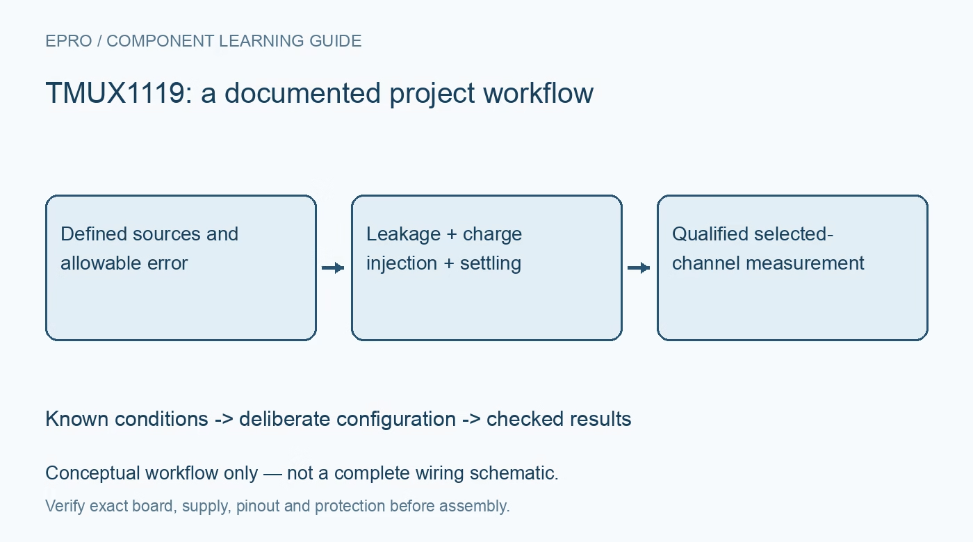
TMUX1119 Precision Switch: 7 Checks for Leakage, Charge Injection and Settling
Plan TMUX1119 precision paths with rail-bounded signals, leakage error budgets, charge-injection recovery and break-before-make timing. This is a documentation-based planning guide, not a report of independent hands-on testing.
1. Map selection without inventing an off state
TMUX1119 is a bidirectional two-to-one analog switch. SEL low connects S1 to D; SEL high connects S2 to D. It has no separate all-off command. Identify the package pinout and the controller reset state before connecting sensitive sources. Both directions can conduct through the selected path, so a destination that can drive voltage must be included in the analysis. Preserve the channel map in firmware and wiring documentation rather than relying on an assumed source-to-drain direction. Manufacturer documentation.
2. Keep analog voltages within the active rails
The supply range is 1.08V to 5.5V, but recommended analog source and drain voltages remain between ground and VDD. The select input has different tolerance rules. A higher-voltage control signal does not permit an analog signal above a lower switch supply. Fail-safe logic protects specified control sequencing; it is not a universal powered-off signal-path guarantee. Build a voltage table covering power-up, steady operation and shutdown, including external pullups and any still-powered sensor connected to the switch. Manufacturer documentation.
3. Convert leakage into an application error
The very-low-leakage headline is useful only with its test conditions and temperature context. Calculate how leakage interacting with source impedance can shift the measured voltage. As an illustration, 3pA through 100 megohms corresponds to 0.3mV; that calculation is not a guaranteed board error. PCB contamination, connectors, humidity and receiver leakage can exceed the switch contribution. Use appropriate cleanliness and guarding, and preserve a realistic worst-case leakage budget instead of treating a room-temperature typical number as a universal maximum. Manufacturer documentation.
4. Treat charge injection as a transient
Selection can disturb the destination through charge injection and parasitic coupling. A small injected charge can produce a large voltage step on a very small capacitance, approximately following voltage change equals charge divided by capacitance. The disturbance also depends on source impedance, signal level and the surrounding network. Inspect the actual transition and recovery before choosing a sample delay. Adding capacitance can reduce the step while extending settling, so evaluate both effects rather than optimizing only the first visible spike. Manufacturer documentation.
Newest in the store


5. Include on-resistance and break-before-make
On-resistance adds to the source and interconnect impedance, affecting loading and the RC acquisition time. Break-before-make briefly disconnects the destination between selections; it avoids intended overlap but does not provide uninterrupted conduction. This matters if the switch sits in a feedback path or a high-impedance hold node. Review how the surrounding circuit behaves while temporarily undriven. The switching-time specification does not replace a measurement of complete source-to-receiver settling at the required accuracy. Manufacturer documentation.
6. Qualify loading with the real receiver active
A switched-capacitor ADC can draw transient current that a high-impedance meter does not reveal. Test the selected source with the intended sampling schedule, filter and acquisition window. Check that dynamic current, voltage and temperature remain within the switch ratings; low resistance does not make this a general-purpose power switch. If a buffer is added, include its input leakage, output settling and stability in the same budget. Compare channel transitions in both directions because source recovery can be asymmetric. Manufacturer documentation.
7. Preserve evidence for the full signal path
Use known bounded sources to compare both channels, repeated transitions and temperature-dependent behavior within the intended operating range. Log supply, source impedance, selection timing, load, settling delay, raw readings and instrument uncertainty. Keep unsettled samples flagged rather than averaging them into plausible values. A useful result is a traceable error budget for one assembled path. This documentation-based workflow does not claim that an arbitrary module achieves the datasheet leakage or precision headline without board-level qualification. Manufacturer documentation.
Related reading: TMUX1219 Analog Switch: 7 Checks for Rail Limits and Break-Before-Make.
Catalog note: The exact-part search did not return a matching Epro listing during preparation. Check the current catalog; this guide makes no price, availability or included-accessory claim.