


TPS62821 Buck Converter: 7 Checks for 1A Limits and Light-Load Behavior

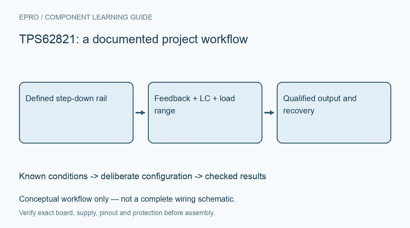
TPS62821 Buck Converter: 7 Checks for 1A Limits and Light-Load Behavior
Review TPS62821 one-amp regulation, effective LC values, light-load mode, dropout, hiccup protection and real PCB thermal limits. This is a documentation-based planning guide, not a report of independent hands-on testing.
1. Use the one-amp member’s specifications
TPS62821 is the 1 A member of a family that also includes higher-current devices. Do not copy the 3 A headline or resistance figures identified specifically with TPS62823. The recommended input range is 2.4 V to 5.5 V and adjustable output range is 0.6 V to 4 V. This is a step-down converter, not a buck-boost source. Check the complete input and load envelope before assuming a chosen output remains regulated throughout battery discharge. Manufacturer documentation.
2. Set the divider and define an output error budget
Use the documented feedback equation and recommended component ranges to select the output divider. Include resistor tolerance, feedback accuracy, ripple and transient deviation in the rail requirement. Route the feedback node according to the layout guidance rather than through a noisy power return. An advertised one-percent feedback accuracy does not independently prove the assembled output stays within one percent under every load transition. Validate the intended voltage at the actual load connection. Manufacturer documentation.
3. Select an effective LC network, not nominal labels
The internally compensated converter is designed for documented inductor and output-capacitor combinations. Check the selection table, inductor saturation and heating, and ceramic capacitance after voltage bias and temperature effects. Keep the input bypass capacitor close to the power pins. Changing inductance or effective capacitance can alter ripple and transient response even when each replacement has an attractive catalog rating. Follow the power-loop layout because a sound component calculation does not eliminate parasitic switching effects. Manufacturer documentation.
4. Expect the frequency to change at light load
The nominal switching frequency is about 2.2 MHz in the relevant operating mode, not a fixed frequency at all loads. Automatic power-save operation reduces switching activity at light load, and the datasheet notes a small output-voltage rise in that mode. Assess ripple and spectral effects against sensitive downstream circuitry. Do not invent a forced-PWM control pin on this device. A low quiescent-current headline also excludes much of the consumption from external dividers and the powered load. Manufacturer documentation.
Newest in the store


5. Understand the limit of one-hundred-percent duty cycle
As input approaches output, the converter can hold the high-side switch on in one-hundred-percent mode. The remaining voltage difference comes from switch and inductor resistance, so output still falls below input by a load-dependent amount. This feature does not create boost operation or preserve the programmed rail below the required headroom. Calculate the minimum usable input at the highest intended current and include wiring and source resistance. Confirm that condition on the assembled board. Manufacturer documentation.
6. Interpret current limiting, hiccup and discharge correctly
The converter limits peak switch current and enters a documented hiccup sequence during sustained overload. That protection is not a precision adjustable current source for the load, and transient peak current can exceed the static threshold because of propagation delay. Review active output discharge and EN behavior before connecting a rail that another source can drive. PG is a status signal with specified thresholds, not proof of zero ripple or immunity to a fast load disturbance. Manufacturer documentation.
7. Verify the real PCB across load and supply extremes
Start with a current-limited source and increase load within the one-amp rating while monitoring voltage, ripple and temperature. Test startup capacitance, light-load transitions, input droop and controlled overload recovery. Use short probe connections so switching pickup is not mistaken for actual rail noise. Record the exact converter, inductor, effective capacitances, ambient conditions and load profile. A family application curve or emissions example cannot establish regulation, thermal margin or compliance for an untested layout. Manufacturer documentation.
Related reading: TPS63060 Buck-Boost Converter: 7 Checks for Real Load Capability.
Catalog note: The exact-part search did not return a matching Epro listing during preparation. Check the current catalog; this guide makes no price, availability or included-accessory claim.