


UCC27611 GaN Gate Driver: 7 Checks for Regulated Drive and Split Outputs

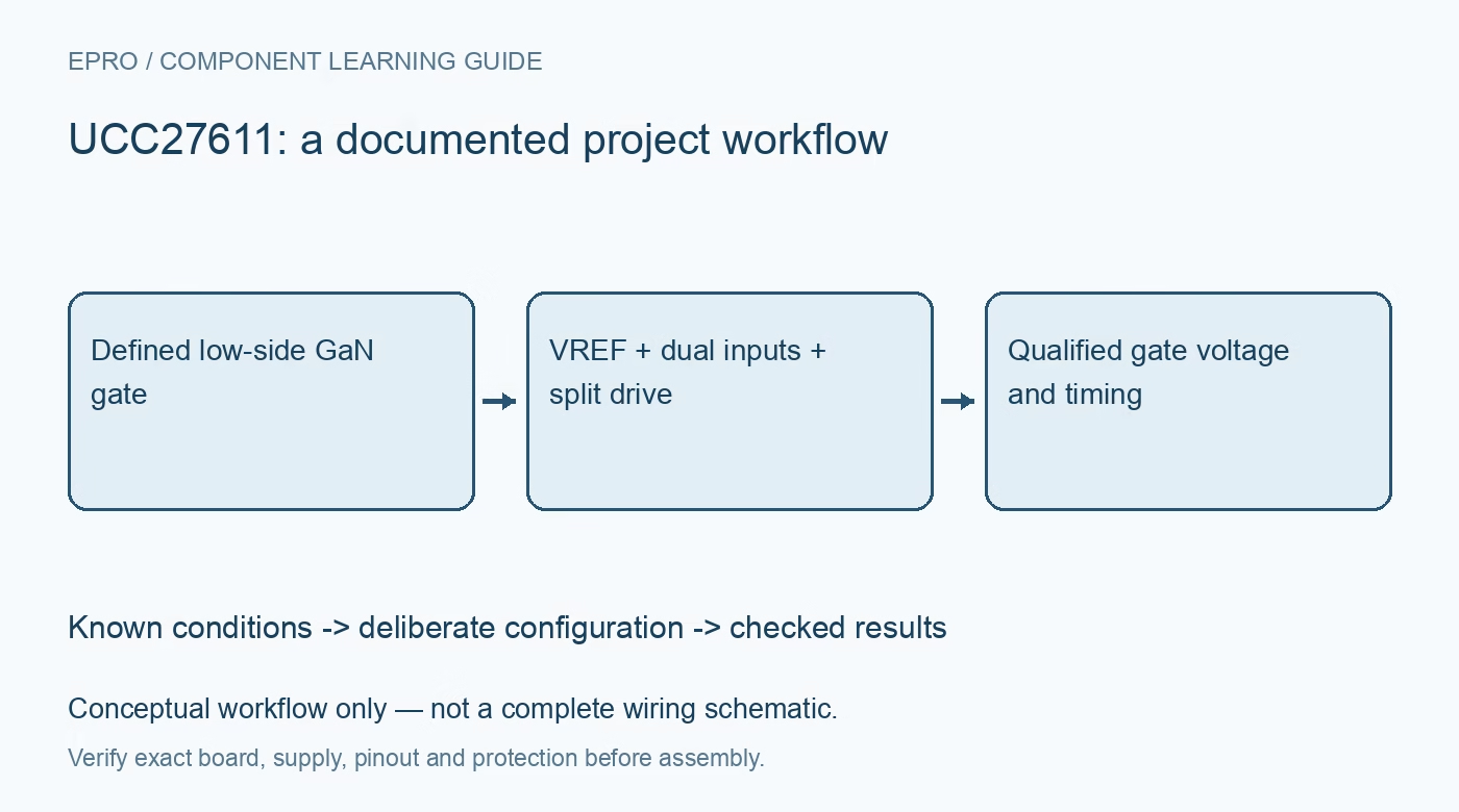
UCC27611 GaN Gate Driver: 7 Checks for Regulated Drive and Split Outputs
Review UCC27611 regulated gate drive, VREF decoupling, dual inputs, split outputs, gate-loop stress and startup behavior. This is a documentation-based planning guide, not a report of independent hands-on testing.
1. Identify a low-side driver with a regulated drive rail
UCC27611 is a single-channel low-side driver intended for enhancement-mode GaN switching devices. Its VDD supply range is 4 V to 18 V, while the internal VREF rail provides nominal five-volt gate drive under the specified regulation conditions. That architecture differs from a conventional driver whose output follows the full supply. Check the transistor gate requirements and reference connection explicitly. The device does not provide high-side level shifting, galvanic isolation or complete power-stage fault management. Manufacturer documentation.
2. Verify VREF rather than assuming five volts everywhere
The internal regulator cannot be treated as an ideal five-volt source at every input voltage and loading condition. Review its output tolerance, line and load regulation, available current and behavior near the lower end of VDD. Measure the actual rail and gate voltage during startup and switching. A transistor with a narrow allowable gate-voltage window still needs margin for tolerance and ringing. Do not use the nominal regulated value as an absolute gate-stress guarantee. Manufacturer documentation.
3. Provide local energy at VDD and VREF
Gate charging draws pulse current through the VREF decoupling network. Follow the manufacturer bypassing recommendations for both supply pins and keep the capacitors close to the driver ground pad. Minimize loop inductance rather than relying on distant bulk capacitance. Returning gate energy can charge the VREF capacitor in an unfavorable layout; the datasheet discusses mitigation for that condition. Any clamp or loading arrangement needs a device-specific review rather than a generic five-volt supply assumption. Manufacturer documentation.
4. Apply both input conditions deliberately
The output is driven high only when IN+ is high and IN− is low. Use IN+ for noninverting PWM with IN− held low, or IN− for inverting operation with IN+ held high. Define the unused input instead of leaving it floating. Internal pull structures hold the output low when inputs float, but external reset states remain important. Compare guaranteed logic thresholds with the controller outputs and account for ground noise during fast switching transitions. Manufacturer documentation.
Newest in the store


5. Use split outputs for controlled gate charging and discharge
OUTH sources gate current and OUTL sinks it, allowing separate turnon and turnoff paths. Route both to the same intended transistor gate through the documented resistor arrangement; they are not independent complementary gate channels. The 4 A source and 6 A sink headlines describe transient capability, not continuous load current. Select resistances from switching loss, overshoot and transistor limits. Increasing edge speed without controlling the loop can increase interference and gate stress. Manufacturer documentation.
6. Qualify the complete gate-current loop
Keep the driver, decoupling, gate resistors and transistor physically close with a deliberate low-side reference return. Measure gate-to-source voltage using suitable low-inductance probing. A long probe ground lead can create misleading ringing, while a poor power return can create genuine unwanted gate excursions. Review transistor source inductance and any permitted reverse-current conditions at the outputs. Start with low stored energy and bounded repetition rate rather than using a high-energy power stage as the first diagnostic fixture. Manufacturer documentation.
7. Verify startup, undervoltage and disable at the gate
The driver includes undervoltage behavior that holds the output low while the necessary supply conditions are inadequate. Observe VDD, VREF, both inputs and the gate during ramps, reset and shutdown. Supply hysteresis and residual stored energy affect timing, so a controller command alone does not establish an instantaneous safe state. Save component values, frequency, gate load and temperature with the waveforms. This planning workflow is not independent bench evidence or a substitute for complete converter protection design. Manufacturer documentation.
Related reading: UCC27516 Gate Driver: 7 Checks for Dual-Input Enable and Gate Stress.
Catalog note: The exact-part search did not return a matching Epro listing during preparation. Check the current catalog; this guide makes no price, availability or included-accessory claim.