


UCC27527 Gate Driver: 7 Checks for Supply-Dependent Logic

UCC27527 Gate Driver: 7 Checks for Supply-Dependent Logic
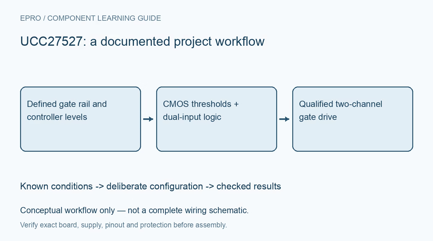
Plan UCC27527 dual gate drive with CMOS thresholds tied to VDD, exact pin mapping, safe default states and controlled timing. This is a documentation-based planning guide, not a report of independent hands-on testing.
1. Identify the dual-input part rather than its sibling
UCC27527 provides two driver channels, each controlled by an inverting and a noninverting input. UCC27528 instead exposes separate enable inputs, and its package pin assignments differ. Verify the exact device before borrowing a symbol or footprint. On UCC27527, VDD is pin five, OUTA pin six and OUTB pin four. A schematic that follows the neighboring device pinout can connect the supply incorrectly even though both parts appear under the same family heading in the manufacturer document. Manufacturer documentation.
2. Calculate the input-high requirement from VDD
The UCC27527 input thresholds are CMOS thresholds that depend on the driver supply voltage. They are not the fixed low-voltage thresholds used by every related gate driver. Review the guaranteed threshold limits, not only the typical switching point, when comparing a controller output with the driver input. Raising VDD to obtain stronger gate enhancement can therefore invalidate the logic interface. Document the worst-case controller high and low levels at the same time as the intended gate-drive supply. Manufacturer documentation.
3. Do not import a dedicated-enable threshold
Each output goes high only with its noninverting input high and its inverting input low. The unused input can implement enable behavior, but it remains an input on this dual-input device. Do not apply the separate-enable threshold specification from UCC27528 to that terminal. Tie the unused input to the documented state when using a simple inverting or noninverting configuration. Include any level translator in the reset-state analysis so both inputs remain valid while its supplies are sequencing. Manufacturer documentation.
4. Match the rail to the transistor and gate network
The driver supply operates from 4.5 V to 18 V, and its output amplitude follows that rail rather than a regulated logic-level output. Check the transistor gate-source rating, required enhancement and allowable negative ringing. The five-ampere source and sink headline describes peak drive into capacitive loads, not continuous power for a general load. Calculate gate-charge demand and switching losses at the intended frequency, then choose external gate resistance and component pulse ratings with the actual transistor in mind. Manufacturer documentation.
Newest in the store


5. Define floating-input and undervoltage behavior intentionally
Internal biasing holds outputs low for floating inputs, and undervoltage lockout also establishes a low output while the rail is inadequate. Those features do not replace a complete startup table for the controller, translators and power stage. Verify the sequence when logic arrives before VDD and when the gate rail remains after the controller powers down. Avoid relying on a floating connection as the normal operating configuration. An externally defined shutdown path is easier to review and reproduce across board revisions. Manufacturer documentation.
6. Separate channel matching from cross-conduction protection
The two channels have closely matched propagation characteristics under specified conditions, but this does not create an interlock or guaranteed system dead time. A pair of commands can still turn on conflicting power switches if the controller or surrounding circuit allows it. Treat this as a low-side, ground-referenced driver without galvanic isolation. Establish dead time and fault response elsewhere when needed, including variations from transistor turn-off, gate resistance and parasitic inductance rather than using a typical channel-delay difference as the whole timing budget. Manufacturer documentation.
7. Inspect both gate loops before energizing the load
Place local bypassing and short gate-return paths according to the package layout guidance. With a current-limited supply, first confirm the logic truth table and gate-source waveforms at a safe representative load. Check each channel independently and then the intended timing relationship, including disable and restart. Probe at the transistor source reference to avoid confusing return-path voltage with gate drive. This documentation-based guide claims no measured switching performance; retain actual waveform evidence before enabling a high-energy power stage. Manufacturer documentation.
Related reading: UCC27526 Dual Gate Driver: 7 Checks for Input Logic and Channel Timing.
Catalog note: The exact-part search did not return a matching Epro listing during preparation. Check the current catalog; this guide makes no price, availability or included-accessory claim.