


TMUX1204 Analog Multiplexer: 7 Checks Before Sharing an ADC

TMUX1204 Analog Multiplexer: 7 Checks Before Sharing an ADC
Use TMUX1204 to share an ADC only after checking rail-bounded inputs, switch resistance, enable polarity and acquisition settling. This is a documentation-based planning guide, not a report of independent hands-on testing.
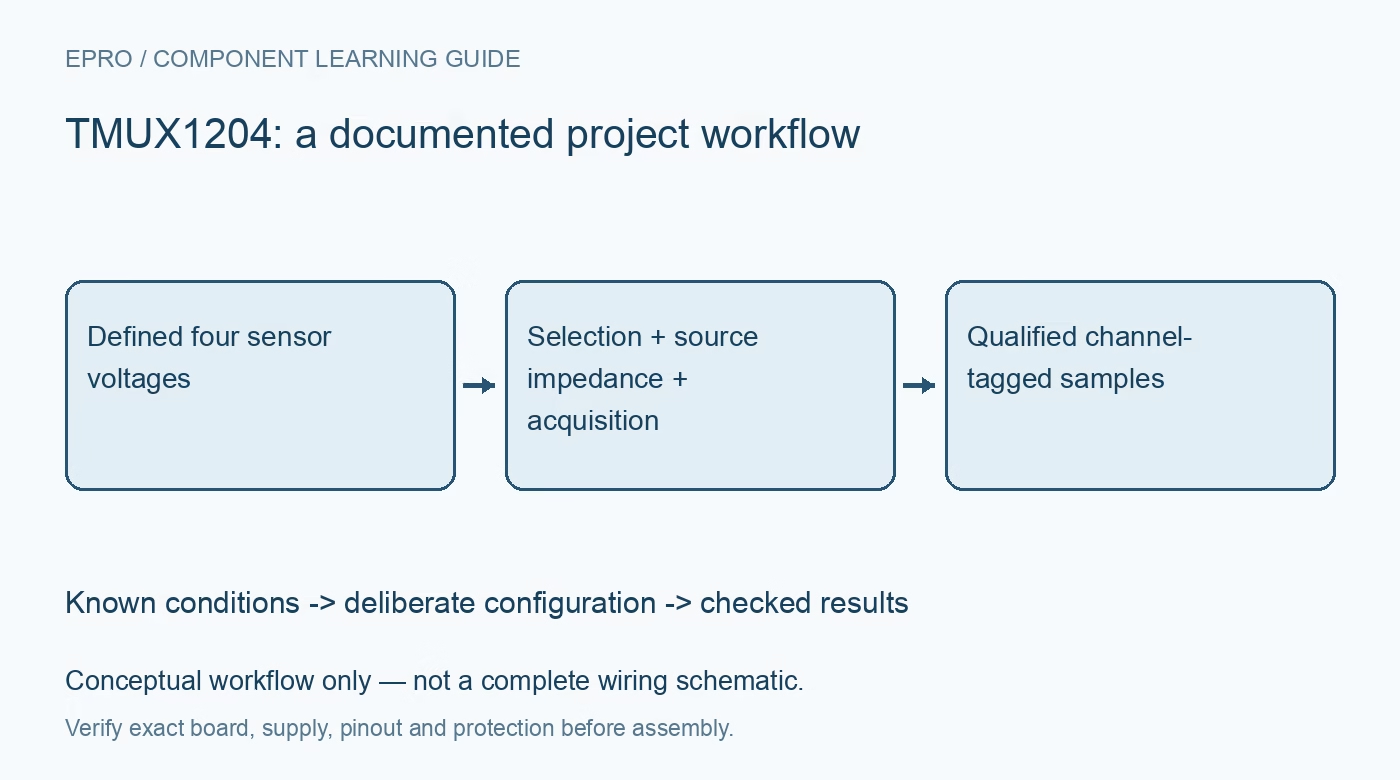
1. Define the four sources and one common destination
TMUX1204 is a single-ended four-to-one analog multiplexer with one common drain. It can route signals bidirectionally, but only the selected path is connected during normal enabled operation. Decide whether the application selects sensor voltages into an ADC or distributes another bounded signal. Label all four sources explicitly in the schematic and software. Do not copy a dual-path multiplexer record format and assume the second signal is being switched by this one-channel device at the same time. Manufacturer documentation.
2. Keep every signal between ground and the supply
The recommended single supply spans 1.08 V to 5.5 V, while the analog path handles signals within ground and VDD. This is not a dual-supply switch for arbitrary bipolar inputs. Include sensor faults and power sequencing when reviewing the minimum and maximum voltage on every source and drain. A source powered from a different rail may remain active after the multiplexer loses power. Absolute-maximum terminal limits describe stress boundaries, not a permitted extended measurement range. Manufacturer documentation.
3. Confirm active-high enable and source numbering
EN low turns all paths off; EN high permits A1 and A0 to select the source. Derive the complete address table from the documentation rather than assuming the numeric label on a connector matches a software array index. Give EN and both address inputs defined reset states. Initially connect safe, distinguishable levels to the sources and verify all four selections. Include the disabled state in the test so an ADC value from a floating common node is not mistaken for a valid disconnected measurement. Manufacturer documentation.
4. Treat on-resistance as a circuit element
The low typical switch resistance is not zero and changes with the operating conditions. In a resistively loaded path it can create gain error; with an ADC it also participates in the acquisition charging path. Combine the appropriate resistance limits with source impedance, input capacitance and any protection or filter resistors. Do not equate a small nominal resistance with precision performance at every signal level. Decide the allowed conversion error before selecting the available settling interval and source drive strength. Manufacturer documentation.
Newest in the store


5. Separate switch transition time from conversion readiness
A fast transition specification describes the switch under its stated test conditions, not the time for an arbitrary sensor and ADC network to reach the required accuracy. Break-before-make behavior also does not remove charge injection or charge left on the common node. Allow for acquisition kickback, previous-channel voltage and load capacitance. Test the largest safe channel-to-channel change and set a sampling policy accordingly, including whether the first conversion after selection should be rejected rather than silently included in an average. Manufacturer documentation.
6. Use fail-safe logic within its stated scope
Fail-safe circuitry applies to the control pins and permits supported logic voltages before VDD is established. It is not a claim that unpowered analog terminals can accept any externally driven sensor voltage. Check partial-power conditions separately for the analog path and the address interface. Provide the documented supply bypassing and appropriate system protection. The device is an analog routing element rather than an isolation barrier, surge protector or buffered sensor interface; those functions need their own design evidence when the installation requires them. Manufacturer documentation.
7. Record channel selection as part of sample quality
Store address, enable state and acquisition timing with each ADC sample. Exercise rapid scanning, long idle periods, a disconnected source and a controller reset while checking that stale data cannot acquire a new channel name. Compare static readings before judging dynamic scanning accuracy. No independent settling or precision measurements are claimed in this article. Keep the accepted source impedance, ADC configuration and timing qualification with the project so changing a sensor or protection resistor triggers a deliberate review rather than an unexplained measurement drift. Manufacturer documentation.
Related reading: TMUX1109 Multiplexer: 7 Checks for Paired Analog Channels.
Catalog note: The exact-part search did not return a matching Epro listing during preparation. Check the current catalog; this guide makes no price, availability or included-accessory claim.