


UCC27526 Dual Gate Driver: 7 Checks for Input Logic and Channel Timing

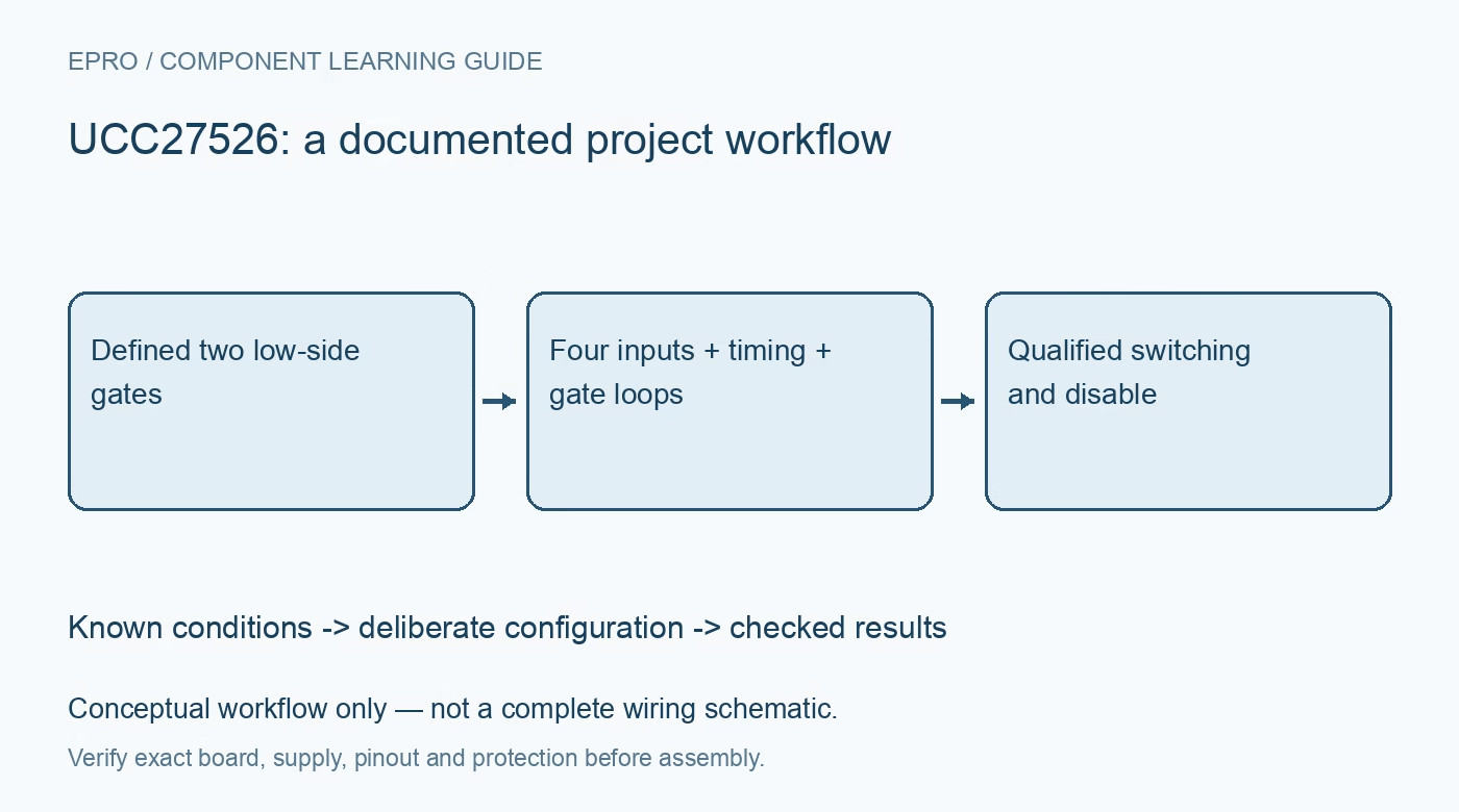
UCC27526 Dual Gate Driver: 7 Checks for Input Logic and Channel Timing
Review UCC27526 dual-input channels, low-side references, gate stress, timing margins, startup behavior and shared thermal demand. This is a documentation-based planning guide, not a report of independent hands-on testing.
1. Identify two low-side channels and four control inputs
UCC27526 contains two independent low-side gate-driver channels, each controlled by a noninverting and an inverting input. Do not substitute the pin functions of another UCC2752x variant that has one input and a separate enable arrangement. Trace both gate outputs, ground and the driver supply against the exact package drawing. Neither channel supplies high-side level shifting or galvanic isolation. The two power switches must have source or emitter references compatible with this low-side architecture. Manufacturer documentation.
2. Apply the same dual-input truth rule to both channels
For either channel, the output becomes high only when its positive input is high and its negative input is low. Holding the negative input low permits noninverting PWM on the positive input; holding the positive input high permits inverting control on the negative input. Define all four inputs during reset and faults. Internal biasing makes floating inputs produce a low output, but it is better to establish deliberate external states than depend on accidental disconnection. Manufacturer documentation.
3. Choose VDD from the transistor gate limits
The driver operates from a recommended 4.5 V to 18 V supply, but the transistor may require a narrower gate-drive range. Include supply tolerance and gate ringing when checking gate-to-source or gate-to-emitter stress. The driver is not a separate gate-voltage regulator. Evaluate guaranteed input thresholds against the controller outputs at their actual supply, rather than treating typical thresholds as logic-margin guarantees. Keep logic return noise and driver power return geometry in the interface review. Manufacturer documentation.
4. Budget gate charge instead of continuous five-amp loads
The 5 A source and sink specification describes brief gate-drive capability into a capacitive load. It does not establish continuous current delivery or the thermal capacity of two simultaneously active channels. Estimate gate-charge demand at the chosen switching frequency and add driver losses. Gate resistance changes peak current, switching loss and electromagnetic interference. A transistor with a larger gate charge can demand substantially more average driver power even if the PWM duty cycle is unchanged. Manufacturer documentation.
Newest in the store


5. Treat delay matching as a specification, not interlocking
The family offers closely matched propagation delays, but it does not automatically insert system dead time or prevent incompatible commands to the two channels. Typical delay matching is not a guaranteed complete timing budget. Include maximum propagation differences, controller timing, transistor turnoff behavior and gate-network tolerances where the power stage needs nonoverlap. Do not infer shoot-through protection from the phrase matched channels. Keep initial tests at low stored energy and verify actual terminal waveforms. Manufacturer documentation.
6. Keep both gate loops compact and decoupling local
Place the driver bypassing close to VDD and ground and minimize each gate-charge loop. Shared return impedance can couple the channels, so keep power-stage current out of the logic reference path. Follow the chosen package thermal and layout guidance. If considering paralleled outputs, use only the documented configuration with identical synchronized commands rather than joining outputs that can disagree. Select probing that measures true gate-to-source voltage without adding a long inductive ground loop. Manufacturer documentation.
7. Check startup, disable and channel interaction together
Observe VDD, both outputs and the relevant control signals during supply ramp, reset and each disable action. Under-voltage lockout holds the outputs low while the supply is inadequate, but that does not prove the whole power stage is de-energized. Test one channel, then simultaneous switching with representative gate loads. Save input states, frequency, gate resistors and temperature observations. A complete verification includes unwanted pulses and ringing, not just a clean-looking steady PWM trace. Manufacturer documentation.
Related reading: UCC27516 Gate Driver: 7 Checks for Dual-Input Enable and Gate Stress.
Catalog note: The exact-part search did not return a matching Epro listing during preparation. Check the current catalog; this guide makes no price, availability or included-accessory claim.