


OPA857 Transimpedance Amplifier: 7 Checks for Gain and Test Modes

OPA857 Transimpedance Amplifier: 7 Checks for Gain and Test Modes
Use OPA857 selectable transimpedance gain only after checking output loading, pseudo-differential reference behavior and normal-versus-test wiring. This is a documentation-based planning guide, not a report of independent hands-on testing.
1. Begin with a dedicated transimpedance architecture
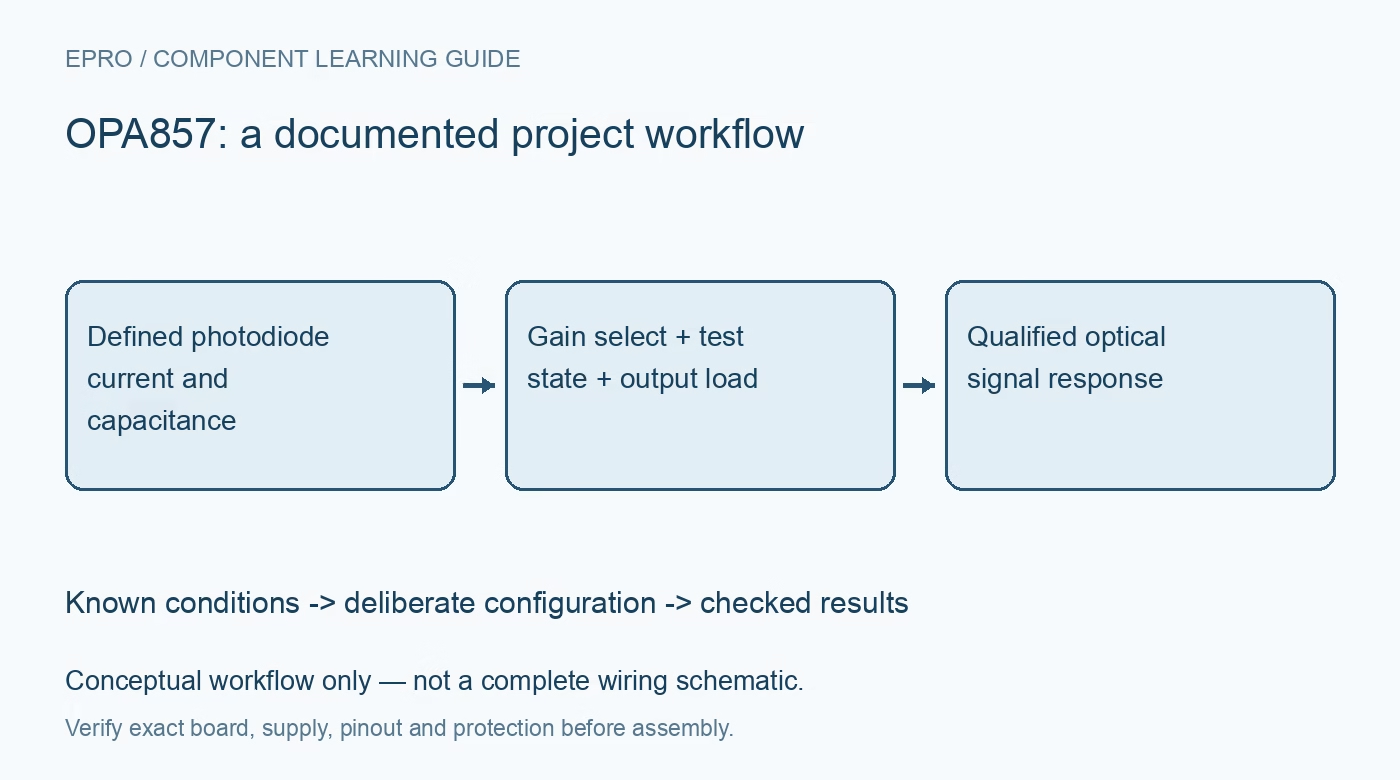
OPA857 is a selectable-feedback transimpedance amplifier rather than a general-purpose voltage amplifier needing an arbitrary external feedback resistor. Its two nominal transimpedance settings are five kilohms and twenty kilohms. Define photodiode polarity, current range and total input capacitance before selecting the gain. The supply range is 2.7 V to 3.6 V, so it is not interchangeable with a higher-voltage laboratory amplifier. Confirm the package and documented input arrangement before connecting a detector or a signal generator. Manufacturer documentation.
2. Give CTRL the intended gain state
CTRL low selects the five-kilohm setting, and CTRL high selects twenty kilohms. The control changes the amplifier configuration, not just a number applied to stored data. Include its default state and any gain changes in the acquisition metadata. Do not switch gain in the middle of an assumed continuous waveform without qualifying the transition and subsequent settling. Check the electrical logic requirements against the actual controller supply so a marginal input level cannot turn a calibration calculation into the wrong transimpedance assumption. Manufacturer documentation.
3. Budget input current against available output swing
The documented signal range is constrained by the internal common-mode level and the class-A output stage. At a 3.3 V supply, the example usable swing is approximately 1.2 V, corresponding to different maximum input currents at the two gain settings. Those are conditional circuit values, not permission to drive the input without checking its limits. Include detector dark current, ambient illumination and pulse peak current when evaluating headroom. A high-gain setting can clip under background current before the desired pulse arrives. Manufacturer documentation.
4. Account for the pseudo-differential output and load
OUT carries the signal and OUTN carries the buffered reference-related output, so the interface is pseudo differential rather than an arbitrary pair of complementary outputs. The reference is derived from five-ninths of the supply. Both output paths include twenty-five-ohm series resistors, which reduce the effective loaded transimpedance. Calculate the attenuation for the actual downstream differential load and amplifier input network. Do not calibrate using an unloaded nominal gain and then assume a terminated measurement cable produces the identical scale factor. Manufacturer documentation.
Newest in the store


5. Select normal and internal-test wiring explicitly
For normal photodiode operation, the documented connections are Test_IN to the positive supply and Test_SD to ground. Test operation uses a different configuration and voltage-to-current structure to emulate an input. A signal generator is not simply connected to the detector input without consideration of bias, current and impedance. Use the manufacturer test-mode procedure and required operating point when exercising that structure. Keep the mode state with the data so a successful electronics test is not mislabeled as a calibrated optical measurement. Manufacturer documentation.
6. Interpret bandwidth and overload recovery conditionally
The headline bandwidth values refer to specific gain and external parasitic capacitance conditions. Additional detector capacitance, board layout and output loading can alter the response. Likewise, fast overload recovery and the internal protection arrangement do not guarantee tolerance of arbitrary external energy. Define pulse amplitude, repetition rate and acceptable recovery before examining the circuit. Use the recommended high-frequency layout and supply bypassing rather than assuming a solderless prototype or long probe lead represents the conditions behind the published performance curves. Manufacturer documentation.
7. Qualify gain, reference and recovery as separate observations
Start with the documented electrical test arrangement, then check normal-mode behavior with the intended detector and safe optical levels. Confirm the reference output, actual loaded scale factor, both gain settings and the return from an over-range event within device limits. Record supply, capacitance, load and measurement bandwidth with the observations. This documentation-based guide reports no independent waveform or noise results. Preserve the distinction between verified electronics operation and a fully calibrated optical signal chain when deciding what the instrument can legitimately report. Manufacturer documentation.
Related reading: OPA859 FET Amplifier: 7 Checks Beyond Unity-Gain Stability.
Catalog note: The exact-part search did not return a matching Epro listing during preparation. Check the current catalog; this guide makes no price, availability or included-accessory claim.