


OPA862 ADC Driver: 7 Checks for Single-Ended to Differential Signals

OPA862 ADC Driver: 7 Checks for Single-Ended to Differential Signals
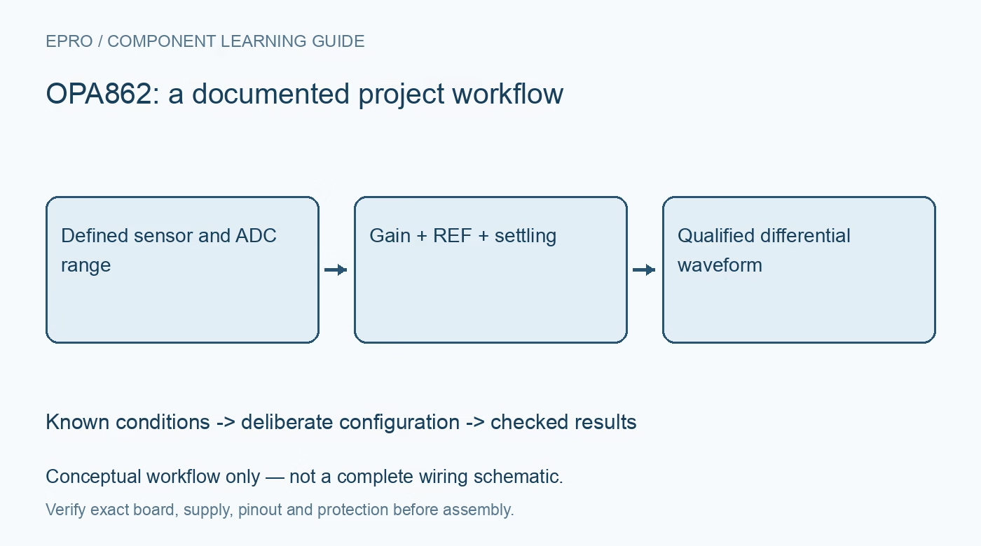
Plan OPA862 gain, REF bias, output headroom and ADC settling without confusing gain-bandwidth product with usable signal bandwidth. This is a documentation-based planning guide, not a report of independent hands-on testing.
1. Identify the intended conversion architecture
The OPA862 is a high-input-impedance, single-ended-to-differential ADC driver. It is not simply two interchangeable general-purpose amplifiers. Begin with the sensor voltage range, source impedance, desired differential swing and receiving ADC input requirements. Draw both output voltages relative to ground as well as their difference. This exposes cases where a reasonable differential amplitude would force one output beyond its linear range. Keep supply and load assumptions attached to that sketch throughout the design review. Manufacturer documentation.
2. Set gain using the documented feedback topology
The device can provide a differential gain of two without external gain-setting resistors in its documented configuration, and other gains use the specified external feedback network. A statement that no gain resistors are required does not mean the feedback pin can be left unconnected. Follow the exact connection diagram and gain equations. Include component tolerance and source loading in the gain budget. Verify a small signal first so clipping cannot hide an incorrect gain definition or swapped differential polarity. Manufacturer documentation.
3. Use REF as an analog operating-point input
REF establishes the output common-mode operating point through the driver architecture. It is not a spare logic input or an unrestricted rail-selection pin. Check its common-mode limits against the selected supplies and the ADC’s required bias. The datasheet specifies headroom relative to both rails rather than permission to choose any supply voltage. Use a suitable low-noise reference path and review bypass guidance. A correct differential amplitude with the wrong output midpoint can still invalidate an ADC measurement. Manufacturer documentation.
4. Budget headroom for each output independently
Calculate the highest and lowest voltage reached by each output under offset, gain and common-mode tolerances. Rail-to-rail output terminology does not mean zero headroom under all loads. Include output current, ADC input transients and any series isolation resistance when checking swing limits. Also verify the input common-mode range independently of output range. Test a modest bounded waveform around the intended bias before exploring full amplitude; otherwise saturation recovery can look like a sampling problem elsewhere in the signal chain. Manufacturer documentation.
Newest in the store


5. Distinguish bandwidth specifications from settling needs
The headline gain-bandwidth product is not the end-to-end bandwidth of every configured signal path. The datasheet lists approximately 44-MHz small-signal bandwidth in its gain-of-two configuration and describes an internal bandwidth-limiting element in the second amplifier. Use the actual response for the chosen topology, not an assumed four-hundred-megahertz flat passband. For an ADC, also assess settling to the required accuracy during acquisition. A fast edge on an oscilloscope does not by itself establish eighteen-bit settling performance. Manufacturer documentation.
6. Review ADC kickback and disable behavior
The receiving converter can impose dynamic capacitive loading that differs substantially from a resistive bench load. Select any output filter and isolation network using the application guidance, then reassess settling and stability. Define the shutdown control level and respect its voltage limits relative to the supplies. Qualification must include recovery after disable, because the first subsequent samples may arrive before the analog path settles. Mark those samples accordingly rather than presenting a low-power mode transition as a transparent continuation of steady-state acquisition. Manufacturer documentation.
7. Validate differential and common-mode behavior together
Measure both outputs with an appropriate probing method and inspect their difference and average. Use a known DC level, a small sine wave and a bounded step under recorded supply and load conditions. Look for common-mode motion, unequal clipping, oscillation and delayed recovery. Retain gain resistors, REF voltage, filter components and ADC timing with the results. Manufacturer distortion and settling specifications describe particular test conditions; this planning guide does not claim that those results were independently reproduced on an unspecified module. Manufacturer documentation.
Related reading: OPA861 OTA: 7 Checks for a Voltage-Controlled Current Stage.
Catalog note: The exact-part search did not return a matching Epro listing during preparation. Check the current catalog; this guide makes no price, availability or included-accessory claim.