


ADS7042 SAR ADC: 7 Checks for Startup Calibration and Supply Scaling

ADS7042 SAR ADC: 7 Checks for Startup Calibration and Supply Scaling
Use ADS7042 data correctly by checking the first-frame calibration, AVDD reference scaling, serial bit alignment and acquisition timing before logging voltage. This is a documentation-based planning guide, not a report of independent hands-on testing.
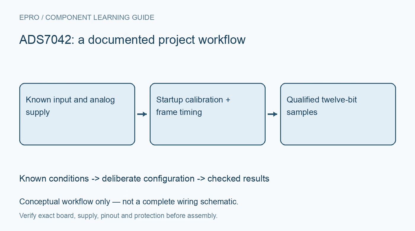
1. Establish the converter and supply arrangement
ADS7042 is a twelve-bit SAR ADC with separate analog and digital supply requirements and a serial interface controlled by chip select and clock. Confirm the package and board schematic before choosing a driver. Unlike an external-reference converter, its analog supply also provides the conversion reference. Record AVDD, DVDD, signal range and host logic levels separately. A nominally compatible SPI controller does not establish valid analog scaling, startup handling or timing for the assembled acquisition chain. Manufacturer documentation.
2. Treat AVDD as part of the measurement
The unipolar input span extends from ground to AVDD under the documented operating conditions. Variation in AVDD therefore changes the volts represented by a conversion code, even when the digital interface is unaffected. Include supply accuracy, noise and dynamic behavior in the error budget, with local bypassing and appropriate return paths. Do not assume a controller’s nominal supply label is an exact reference measurement. Check the input at the ADC pins and keep it within the applicable operating and absolute limits. Manufacturer documentation.
3. Handle the first transfer as calibration, not a sample
After power-up, the first chip-select falling edge initiates internal offset calibration. The datasheet requires chip select to remain low for at least sixteen serial-clock falling edges to complete that process, and the data output stays low during the initial transfer. Do not log this all-zero frame as a measured zero-volt input. Follow the documented clock limits for the actual analog supply and provide the required acquisition interval before accepting the first conversion result. Manufacturer documentation.
4. Separate ordinary frames from deliberate recalibration
Normal conversion frames and the longer sequence used for offset calibration during operation have different consequences. The datasheet describes recalibration when at least thirty-two clock falling edges occur within the applicable frame. Check the host driver’s actual clock count, including padding, rather than assuming additional clocks are always harmless. If recalibration is intended, schedule it explicitly and respect the recovery and acquisition requirements. Internal offset calibration does not calibrate the external sensor, supply reference, gain error or complete measurement system. Manufacturer documentation.
Newest in the store


5. Align twelve data bits after the leading zeros
The serial output starts with two zero bits followed by the twelve conversion bits; later clock behavior and chip-select release are defined by the timing diagram. Extract the correct field rather than treating an arbitrary received word as an unshifted twelve-bit result. Verify clock-edge selection and the interval between chip-select assertion and clock activity. Use synthetic bit patterns in the parser and a known bounded input on hardware so leading zeros cannot disguise a framing mistake as a small real signal. Manufacturer documentation.
6. Budget analog settling and sampling cadence together
The input sample-and-hold needs a source that settles within the available acquisition interval. Evaluate source impedance, any filter, input changes and sample rate as a complete chain. No data latency does not mean zero conversion time, unlimited bandwidth or immediate recovery from a supply change. Observe representative operation at the intended fastest sampling schedule. Lower average power at a slower rate is useful, but does not prove that the input or analog supply behaves correctly during a burst of conversions. Manufacturer documentation.
7. Preserve calibration and scaling context in the log
Compare settled results with several known input levels and suitable reference equipment. Save raw frames, extracted codes, AVDD, DVDD, clock settings, acquisition interval and the events that trigger startup or recalibration. Mark calibration frames and acquisition interruptions as invalid measurements rather than silently averaging them into a dataset. This documentation-based guide defines checks, not independent converter test results. Revisit the evidence after changing the host transfer width, power-cycling schedule, analog supply or source network. Manufacturer documentation.
Related reading: ADS8326 SAR ADC: 7 Checks for Clocked Acquisition and Unsigned Codes.
Catalog note: The exact-part search did not return a matching Epro listing during preparation. Check the current catalog; this guide makes no price, availability or included-accessory claim.