


ADS7056 SAR ADC: 7 Checks for 14-Bit Frames and Previous-Sample Identity

ADS7056 SAR ADC: 7 Checks for 14-Bit Frames and Previous-Sample Identity
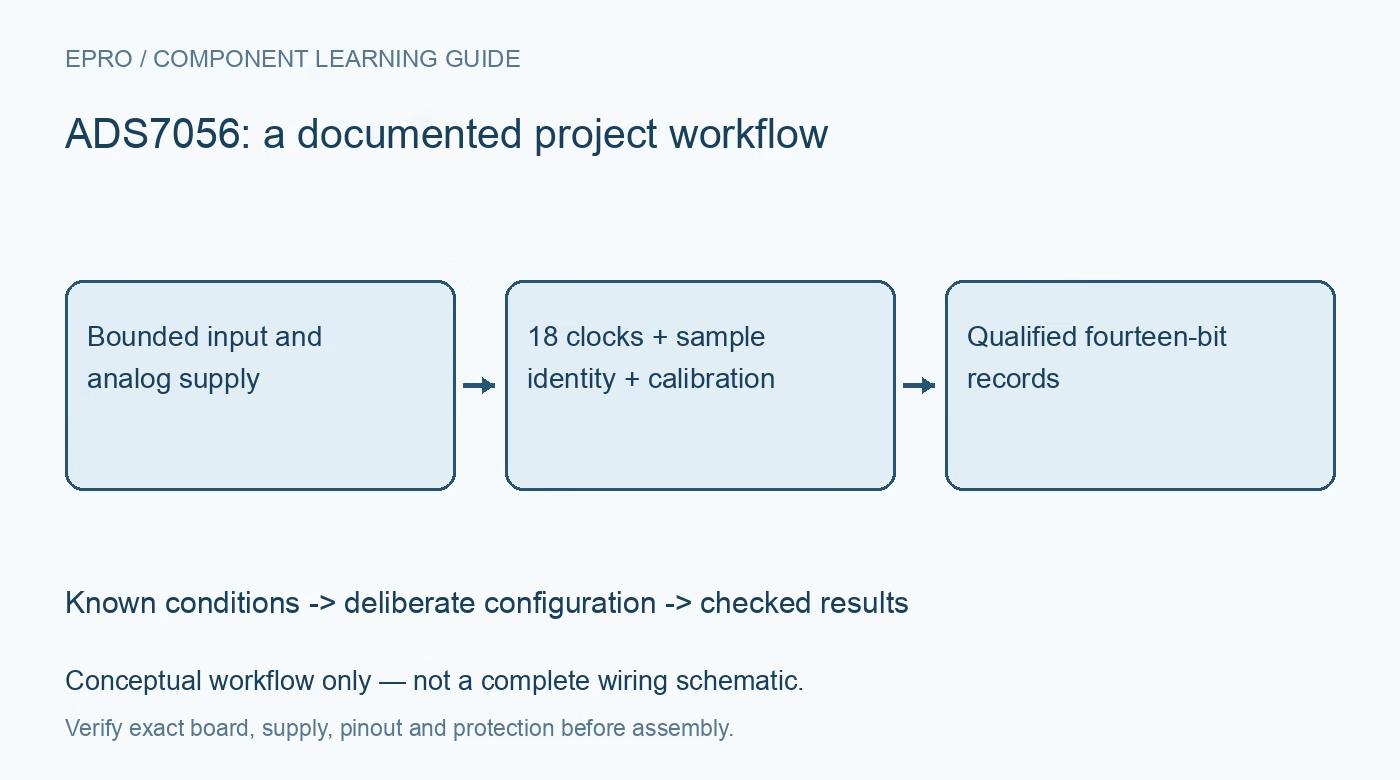
Qualify ADS7056 14-bit sampling with AVDD referencing, 18-clock conversions, previous-sample framing and distinct startup calibration timing. This is a documentation-based planning guide, not a report of independent hands-on testing.
1. Define the analog and digital supply domains
The ADS7056 is a 14-bit SAR converter with separate analog and digital supplies. AVDD operates from 2.35 to 3.6 volts, while DVDD operates from 1.65 to 3.6 volts. AVDD also establishes the conversion reference, so its error and disturbance directly affect the reported scale. Specify both rails and their decoupling, not merely the microcontroller logic voltage. Check the exact package connections and return paths before applying a signal; a digital interface that responds correctly does not validate the analog supply quality. Manufacturer documentation.
2. Keep the negative input near its specified reference
The differential full-scale span is zero to AVDD, but AINM is not an unrestricted bipolar or rail-to-rail companion input. The electrical table constrains AINM to within 0.1 volt of ground under its stated conditions. Do not connect a floating differential source anywhere inside the supply rails and expect valid conversion. Bound both terminal voltages, source impedance and transient behavior. Begin with a known low-voltage source referenced correctly, leaving margin from the endpoints while checking basic scale and offset. Manufacturer documentation.
3. Track sampling separately from serial readout
A falling edge on CS samples the next analog value and starts conversion. The serial bits shifted out in that frame belong to the previous conversion, not the just-sampled input. The first frame after power-up supplies zeros rather than a qualified first measurement. Associate each received word with the correct earlier sample time in firmware. Use a controlled input transition to check the one-frame relationship; a constant voltage can hide an indexing mistake that later corrupts synchronized measurements. Manufacturer documentation.
4. Preserve eighteen conversion clocks and bit alignment
Normal conversion requires at least eighteen SCLK falling edges within the frame, even though the result contains fourteen data bits. The serial output begins with a leading zero, followed by D13 through D0 according to the documented launch edges, then zeros. Providing fewer than eighteen falling edges invalidates the next frame result. Capture CS, SCLK and SDO together and verify bit extraction explicitly. Do not assume a convenient sixteen-clock SPI transaction completes the analog conversion merely because fourteen data bits were visible. Manufacturer documentation.
Newest in the store


5. Distinguish startup calibration from later calibration
At power-up, the host must provide twenty-four clocks in the first serial transfer for the documented offset-calibration sequence. During normal operation, calibration instead uses a sixty-four-clock frame, whose early output still contains the previous result. These are not interchangeable recipes. Pulling CS high too early aborts the calibration process. Reserve the required acquisition interval afterward, and mark calibration periods in the data stream. Offset correction does not remove gain error, reference variation or errors in the external signal path. Manufacturer documentation.
6. Budget acquisition and source settling at the chosen rate
The converter headline is up to 2.5 million samples per second, with a serial clock specification up to 60 megahertz under the documented conditions. A valid cycle also includes conversion and the minimum 95-nanosecond acquisition period; clock frequency alone does not establish throughput. The switched sampling input must settle from the actual source impedance and filter network. Review driver stability and charge demand before increasing rate. Check accuracy against a defined error criterion rather than equating a fourteen-bit word with fourteen noise-free bits. Manufacturer documentation.
7. Save sample identity and integrity checks with the data
Log raw words, extraction format, sample timestamps, frame counts, supply values and calibration events. Use known bounded inputs at several levels and inspect both static error and repeated-sample spread. Identify dropped host transfers or timing interruptions explicitly; do not invent a CRC or ready flag that the device does not provide. Keep documentation-derived expectations separate from bench measurements. A trustworthy record shows which physical sample each value represents and why its frame was accepted, not simply a stream of plausible decimal voltages. Manufacturer documentation.
Related reading: ADS7052 SAR ADC: 7 Checks for Previous-Sample Data and Calibration.
Catalog note: The exact-part search did not return a matching Epro listing during preparation. Check the current catalog; this guide makes no price, availability or included-accessory claim.